
- English
- Español
- Português
- русский
- Français
- 日本語
- Deutsch
- tiếng Việt
- Italiano
- Nederlands
- ภาษาไทย
- Polski
- 한국어
- Svenska
- magyar
- Malay
- বাংলা ভাষার
- Dansk
- Suomi
- हिन्दी
- Pilipino
- Türkçe
- Gaeilge
- العربية
- Indonesia
- Norsk
- تمل
- český
- ελληνικά
- український
- Javanese
- فارسی
- தமிழ்
- తెలుగు
- नेपाली
- Burmese
- български
- ລາວ
- Latine
- Қазақша
- Euskal
- Azərbaycan
- Slovenský jazyk
- Македонски
- Lietuvos
- Eesti Keel
- Română
- Slovenski
- मराठी
- Srpski језик
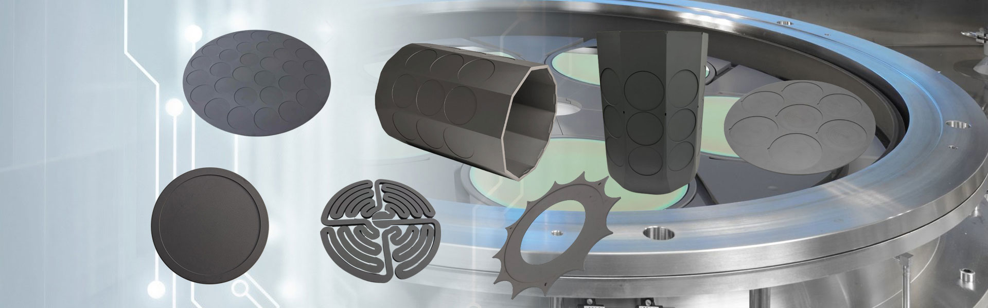


Etching Wafer Carrier
Semicorex Etching Wafer Carrier with CVD SiC Coating is an advanced, high-performance solution tailored for demanding semiconductor etching applications. Its superior thermal stability, chemical resistance, and mechanical durability make it an essential component in modern wafer fabrication, ensuring high efficiency, reliability, and cost-effectiveness for semiconductor manufacturers worldwide.*
Send Inquiry
Product Description
Semicorex Etching Wafer Carrier is a high-performance substrate support platform designed for semiconductor fabrication processes, specifically for wafer etching applications. Engineered with a high-purity graphite base and coated with Chemical Vapor Deposition (CVD) Silicon Carbide (SiC), this wafer carrier provides exceptional chemical resistance, thermal stability, and mechanical durability, ensuring optimal performance in high-precision etching environments.
The Etching Wafer Carrier is coated with a uniform CVD SiC layer, which significantly enhances its chemical resistance against aggressive plasma and corrosive gases used in the etching process. CVD is the main technology for preparing SiC coating on substrate surface at present. The main process is that the gas phase reactant raw materials undergo a series of physical and chemical reactions on the substrate surface, and finally deposit on the substrate surface to prepare SiC coating. The SiC coating prepared by CVD technology is closely bonded to the substrate surface, which can effectively improve the oxidation resistance and ablation resistance of the substrate material, but the deposition time of this method is long, and the reaction gas contains certain toxic gases.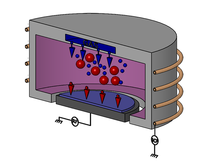
CVD silicon carbide coating parts are widely used in etching equipment, MOCVD equipment, Si epitaxial equipment and SiC epitaxial equipment, rapid thermal processing equipment and other fields. Overall, the largest market segment of CVD silicon carbide coating parts is etching equipment and epitaxial equipment parts. Due to the low reactivity and conductivity of CVD silicon carbide coating to chlorine-containing and fluorine-containing etching gases, it becomes an ideal material for focusing rings and other parts of plasma etching equipment. CVD SiC parts in etching equipment include focusing rings, gas shower heads, trays, edge rings, etc. Take the focus ring as an example. The focus ring is an important component placed outside the wafer and in direct contact with the wafer. Voltage is applied to the ring to focus the plasma passing through the ring, thereby focusing the plasma on the wafer to improve processing uniformity. Traditional focus rings are made of silicon or quartz. With the advancement of integrated circuit miniaturization, the demand and importance of etching processes in integrated circuit manufacturing are increasing, and the power and energy of etching plasma continue to increase.
The SiC coating offers superior resistance against fluorine-based (F₂) and chlorine-based (Cl₂) plasma etching chemistries, preventing degradation and maintaining structural integrity over prolonged use. This chemical robustness ensures consistent performance and reduces contamination risks during wafer processing. The wafer carrier can be tailored to various wafer sizes (e.g., 200mm, 300mm) and specific etching system requirements. Custom slot designs and hole patterns are available to optimize wafer positioning, gas flow control, and process efficiency.
Applications and Benefits
The Etching Wafer Carrier is primarily used in semiconductor manufacturing for dry etching processes, including Plasma Etching (PE), Reactive Ion Etching (RIE), and Deep Reactive Ion Etching (DRIE). It is widely adopted in the production of integrated circuits (ICs), MEMS devices, power electronics, and compound semiconductor wafers. Its robust SiC coating ensures consistent etching results by preventing material degradation. The combination of graphite and SiC provides long-term durability, reducing maintenance and replacement costs. The smooth and dense SiC surface minimizes particle generation, ensuring high wafer yield and superior device performance. Exceptional resistance to harsh etching environments reduces the need for frequent replacements, improving manufacturing efficiency.
Hot Tags: Etching Wafer Carrier, China, Manufacturers, Suppliers, Factory, Customized, Bulk, Advanced, Durable
Product Tag
Related Category
Si Epitaxy
SiC Epitaxy
MOCVD Susceptor
PSS Etching Carrier
ICP Etching Carrier
RTP Carrier
LED Epitaxial Susceptor
Barrel Susceptor
Monocrystalline Silicon
Pancake Susceptor
Photovoltaic Parts
GaN on SiC Epitaxy
Send Inquiry
Please feel free to give your inquiry in the form below. We will reply you in 24 hours.


