
- English
- Español
- Português
- русский
- Français
- 日本語
- Deutsch
- tiếng Việt
- Italiano
- Nederlands
- ภาษาไทย
- Polski
- 한국어
- Svenska
- magyar
- Malay
- বাংলা ভাষার
- Dansk
- Suomi
- हिन्दी
- Pilipino
- Türkçe
- Gaeilge
- العربية
- Indonesia
- Norsk
- تمل
- český
- ελληνικά
- український
- Javanese
- فارسی
- தமிழ்
- తెలుగు
- नेपाली
- Burmese
- български
- ລາວ
- Latine
- Қазақша
- Euskal
- Azərbaycan
- Slovenský jazyk
- Македонски
- Lietuvos
- Eesti Keel
- Română
- Slovenski
- मराठी
- Srpski језик


China CVD SiC Manufacturers, Suppliers, Factory
CVD SiC is a vacuum deposition process used to produce high-purity solid materials. This process is often used in semiconductor manufacturing to form thin films on wafer surfaces. During the chemical vapor deposition (CVD) process for producing silicon carbide (SiC), a substrate is exposed to one or more volatile precursors, which chemically react on the substrate surface to form the desired SiC deposit. Among the various methods for producing SiC, CVD produces products with high uniformity and purity, and offers strong process controllability.
Simply put, CVD SiC refers to SiC produced via the chemical vapor deposition (CVD) process. In this process, gaseous precursors, typically containing silicon and carbon, react in a high-temperature reactor to deposit a thin SiC film onto a substrate. CVD SiC is valued for its exceptional properties, including high thermal conductivity, chemical inertness, mechanical strength, and resistance to thermal shock and wear. These properties make chemical vapor deposited (CVD) silicon carbide (SiC) ideal for demanding applications such as semiconductor manufacturing, aerospace components, armor, and high-performance coatings. This material's exceptional durability and stability under extreme conditions ensure its effectiveness in improving the performance and lifespan of advanced technologies and industrial systems.
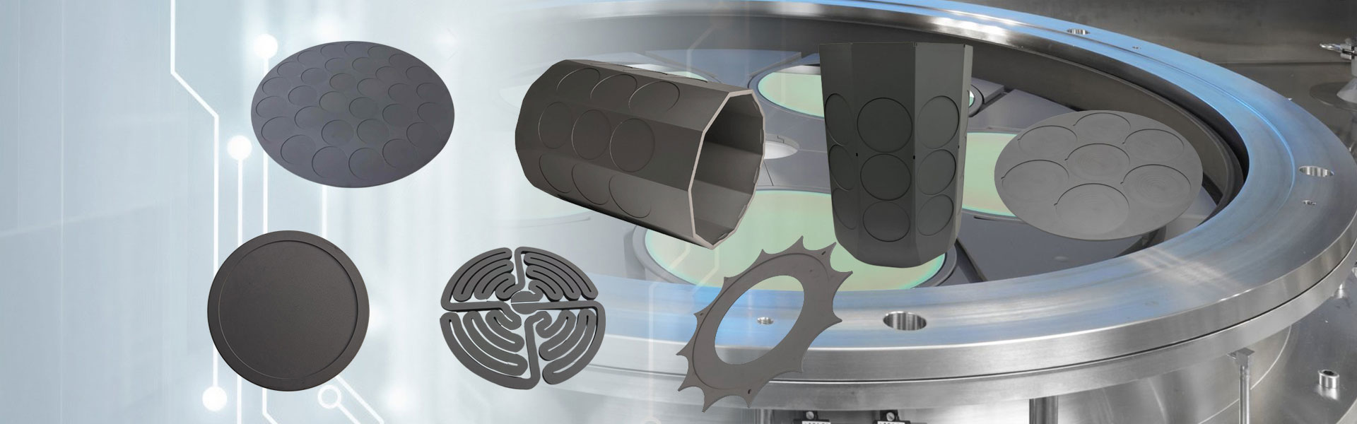
CVD SiC materials, due to their unique combination of excellent thermal, electrical, and chemical properties, are well-suited for applications in the semiconductor industry, where high-performance materials are required. Chemical vapor deposited (CVD) silicon carbide (SiC) components are widely used in etching equipment, MOCVD equipment, Si and SiC epitaxy equipment, and rapid thermal processing equipment.
The largest market segment for CVD SiC components is etching equipment components. Due to its low reactivity to chlorine- and fluorine-containing etching gases and its electrical conductivity, CVD silicon carbide (SiC) is an ideal material for components such as focus rings in plasma etching equipment. CVD silicon carbide (SiC) components in etching equipment include focus rings, gas showerheads, trays, edge rings.
Take the focus ring, for example. This critical component is placed outside the wafer and in direct contact with it. Voltage is applied to the ring to focus the plasma passing through it, thereby focusing the plasma on the wafer and improving processing uniformity. Traditionally, focus rings are made of silicon or quartz. However, with the advancement of integrated circuit miniaturization, the demand for and importance of etching processes in integrated circuit manufacturing continues to increase. The power and energy of the plasma used for etching are also increasing, especially in capacitively coupled plasma (CCP) etching equipment, which requires even higher plasma energies. Consequently, focus rings made of silicon carbide are becoming increasingly popular.
Due to the high performance of CVD SiC and its ability to be sliced into very thin sections, it can also benefit sputter targets and all types of electrodes.
Process of Chemical Vapor Deposition (CVD)
CVD is a process that transforms a material from a gas phase to a solid phase, used to form a thin film or coating on a substrate surface. The following are the basic steps in CVD:
1. Substrate Preparation
Choose an appropriate substrate material and perform the appropriate cleaning and surface treating to produce a clean, flat surface with good adhesion.
2. Reactive Gas Preparation
Prepare the necessary amount of reactive gas or vapor and inject it into the deposition chamber by some means (gas supply system). The reactive gas can be an organic compound, a metal-organic precursor, inert gas, or other gaseous species.
3. Deposition Reaction
If all instrumentation is setup correctly the CVD process will begin under the pre-defined reaction conditions. The reactive gas that has been injected into the chamber will undergo some chemical or physical reaction on the substrate surface to form a deposit onto the substrate surface. The deposit formation can be the result of several types of processes depending on the deposition method, these include vapor-phase thermal decomposition, chemical reaction, sputtering, epitaxial growth, etc.
4. Control and Monitoring
At the same time during the deposition process, certain deposition parameters need to be controlled and monitored in real time if the observer wishes to ensure the best possible properties in the film are maintained. These include relevant temperature measurement, pressure monitoring, and regulation of gas flow, all the while aiming to keep the desired reaction conditions stable and constant.
5. Deposition Completion and Post-Processing
When either the deposition time, predetermined thickness, or method selected, is achieved the introduction of the reaction gas can be ceased and deposition process ended. Following the deposition, several pertinent post-processing methods (annealing, structural modifications, surface treatment, etc.) should be performed to improve the film performance/quality.
It's important to note that the specific vapor deposition process can vary depending on the deposition technology, material type, and application requirements. However, the basic process outlined above covers most common vapor deposition steps.
- View as

CVD SiC Shower heads
Semicorex CVD SiC Shower Heads are high-purity, precision-engineered component designed for CCP and ICP etching systems in advanced semiconductor manufacturing. Choosing Semicorex means gaining reliable solutions with superior material purity, machining accuracy, and durability for the most demanding plasma processes.*
Read MoreSend Inquiry
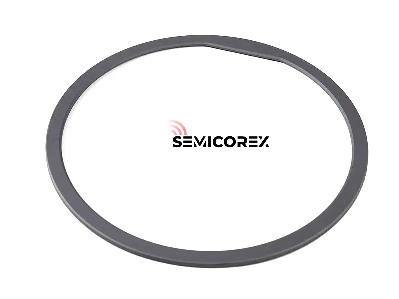
Edge Rings
Semicorex Edge Rings are trusted by leading semiconductor fabs and OEMs worldwide. With strict quality control, advanced manufacturing processes, and application-driven design, Semicorex provides solutions that extend tool life, optimize wafer uniformity, and support advanced process nodes.*
Read MoreSend Inquiry
Gas Distribution Plates
Semicorex Gas Distribution Plates, made of CVD SiC is a critical component in plasma etching systems, designed to ensure uniform gas dispersion and consistent plasma performance across the wafer. Semicorex is the trusted choice for high-performance ceramic solutions, offering unmatched material purity, engineering precision, and dependable support tailored to the demands of advanced semiconductor manufacturing.*
Read MoreSend Inquiry
Solid SiC Shower Head
The Solid SiC Shower Head is a crucial component in semiconductor manufacturing, specifically designed for chemical vapor deposition (CVD) processes. Semicorex, a leader in advanced materials technology, offers Solid SiC Shower Heads that ensure superior distribution of precursor gases over substrate surfaces. This precision is vital for achieving high-quality and consistent processing results.**
Read MoreSend Inquiry
CVD SiC Focus Ring
Through a process of chemical vapor deposition (CVD), Semicorex CVD SiC Focus Ring is meticulously deposited and mechanically processed to achieve the final product. With its superior material properties, it's indispensable in the demanding environments of modern semiconductor fabrication.**
Read MoreSend Inquiry
Etching Ring
The Etching Ring made of CVD SiC is an essential component in the semiconductor manufacturing process, offering exceptional performance in plasma etching environments. With its superior hardness, chemical resistance, thermal stability, and high purity, CVD SiC ensures that the etching process is precise, efficient, and reliable. By choosing Semicorex CVD SiC Etching Rings, semiconductor manufacturers can enhance the longevity of their equipment, reduce downtime, and improve the overall quality of their products.*
Read MoreSend Inquiry
Semicorex has been producing CVD SiC for many years and is one of the professional CVD SiC manufacturers and Suppliers in China. Once you buy our advanced and durable products which supply bulk packing, we guarantee the large quantity in quick delivery. Over the years, we have provided customers with customized service. Customers are satisfied with our products and excellent service. We sincerely look forward to becoming your reliable long-term business partner! Welcome to buy products from our factory.


