
- English
- Español
- Português
- русский
- Français
- 日本語
- Deutsch
- tiếng Việt
- Italiano
- Nederlands
- ภาษาไทย
- Polski
- 한국어
- Svenska
- magyar
- Malay
- বাংলা ভাষার
- Dansk
- Suomi
- हिन्दी
- Pilipino
- Türkçe
- Gaeilge
- العربية
- Indonesia
- Norsk
- تمل
- český
- ελληνικά
- український
- Javanese
- فارسی
- தமிழ்
- తెలుగు
- नेपाली
- Burmese
- български
- ລາວ
- Latine
- Қазақша
- Euskal
- Azərbaycan
- Slovenský jazyk
- Македонски
- Lietuvos
- Eesti Keel
- Română
- Slovenski
- मराठी
- Srpski језик
China Wafer Manufacturers, Suppliers, Factory
What is the semiconductor wafer?
A semiconductor wafer is a thin, round slice of semiconductor material that serves as the foundation for the fabrication of integrated circuits (ICs) and other electronic devices. The wafer provides a flat and uniform surface on which various electronic components are built.
The wafer manufacturing process involves several steps, including growing a large single crystal of the desired semiconductor material, slicing the crystal into thin wafers using a diamond saw, and then polishing and cleaning the wafers to remove any surface defects or impurities. The resulting wafers have a highly flat and smooth surface, which is crucial for the subsequent fabrication processes.
Once the wafers are prepared, they undergo a series of semiconductor manufacturing processes, such as photolithography, etching, deposition, and doping, to create the intricate patterns and layers required to build electronic components. These processes are repeated multiple times on a single wafer to create multiple integrated circuits or other devices.
After the fabrication process is complete, the individual chips are separated by dicing the wafer along predefined lines. The separated chips are then packaged to protect them and provide electrical connections for integration into electronic devices.
Different materials on wafer
Semiconductor wafers are primarily made from single-crystal silicon due to its abundance, excellent electrical properties, and compatibility with standard semiconductor manufacturing processes. However, depending on specific applications and requirements, other materials can also be used to make wafers. Here are some examples:
Silicon Carbide (SiC): SiC is a wide-bandgap semiconductor material known for its excellent thermal conductivity and high-temperature performance. SiC wafers are used in high-power electronic devices, such as power converters, inverters, and electric vehicle components.
Gallium Nitride (GaN): GaN is a wide-bandgap semiconductor material with exceptional power handling capabilities. GaN wafers are used in the production of power electronic devices, high-frequency amplifiers, and LEDs (light-emitting diodes).
Gallium Arsenide (GaAs): GaAs is another common material used for wafers, particularly in high-frequency and high-speed applications. GaAs wafers offer better performance for certain electronic devices, such as RF (radio frequency) and microwave devices.
Indium Phosphide (InP): InP is a material with excellent electron mobility and is often used in optoelectronic devices like lasers, photodetectors, and high-speed transistors. InP wafers are suitable for applications in fiber-optic communication, satellite communication, and high-speed data transmission.


- View as

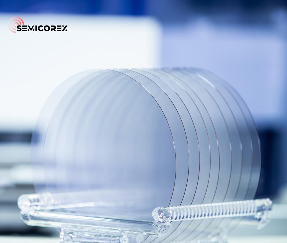
Glass Wafers
Semicorex glass wafers are circular thin slices made from semiconductor-grade glass. Due to their exceptional high-temperature resistance, strength corrosion resistance, excellent mechanical properties, and high light transmission efficiency, they are widely used in precision manufacturing fields such as semiconductors, optics, biotechnology, microelectronics, and integrated circuit (IC) packaging.
Read MoreSend Inquiry
SICOI Wafer
SICOI wafer, a silicon carbide-insulator composite wafer made by a special technique, is primarily utilized in photonic integrated circuits and microelectromechanical systems (MEMS). This composite structure combines the excellent properties of silicon carbide with the isolation characteristics of insulators, significantly enhancing the overall performance of semiconductor devices and providing ideal solutions for high-performance electronic and optoelectronic devices.
Read MoreSend Inquiry
Monocrystalline Silicon Wafers
Monocrystalline silicon wafers, crafted by the excellent high-purity monocrystalline silicon, offer exceptional flatness, low defect density, and superior quality. Semicorex prioritizes customer needs and is committed to providing premium wafer solutions required for advanced semiconductor industry.
Read MoreSend Inquiry
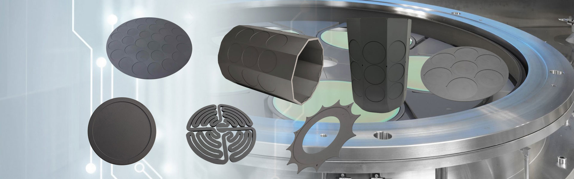
PFA Wafer Cassettes
Semicorex PFA Wafer Cassettes are high-purity carriers designed to ensure safe and contamination-free handling of semiconductor wafers during wet processing, storage, and transport. Choosing Semicorex guarantees not only superior PFA material quality but also precision engineering that delivers reliability, cleanliness, and long-term performance in advanced fabrication environments.*
Read MoreSend Inquiry
PFA Wafer Carriers
Semicorex PFA Wafer Carriers are high-purity, chemically resistant solution designed to safely handle and transport semiconductor wafers in ultra-clean environments. Trusted by leading fabs and OEMs, Semicorex delivers precision-engineered carriers with consistent quality, fast lead times, and full customization to meet the evolving demands of advanced semiconductor manufacturing.*
Read MoreSend Inquiry
Teflon Cassettes
Semicorex Teflon Cassettes are high-purity PTFE wafer carriers designed for safe, contamination-free processing in corrosive chemical environments. Choose Semicorex for industry-leading precision, reliable quality, and customizable solutions backed by expertise in semiconductor handling systems.*
Read MoreSend Inquiry
Semicorex has been producing Wafer for many years and is one of the professional Wafer manufacturers and Suppliers in China. Once you buy our advanced and durable products which supply bulk packing, we guarantee the large quantity in quick delivery. Over the years, we have provided customers with customized service. Customers are satisfied with our products and excellent service. We sincerely look forward to becoming your reliable long-term business partner! Welcome to buy products from our factory.


