
- English
- Español
- Português
- русский
- Français
- 日本語
- Deutsch
- tiếng Việt
- Italiano
- Nederlands
- ภาษาไทย
- Polski
- 한국어
- Svenska
- magyar
- Malay
- বাংলা ভাষার
- Dansk
- Suomi
- हिन्दी
- Pilipino
- Türkçe
- Gaeilge
- العربية
- Indonesia
- Norsk
- تمل
- český
- ελληνικά
- український
- Javanese
- فارسی
- தமிழ்
- తెలుగు
- नेपाली
- Burmese
- български
- ລາວ
- Latine
- Қазақша
- Euskal
- Azərbaycan
- Slovenský jazyk
- Македонски
- Lietuvos
- Eesti Keel
- Română
- Slovenski
- मराठी
- Srpski језик


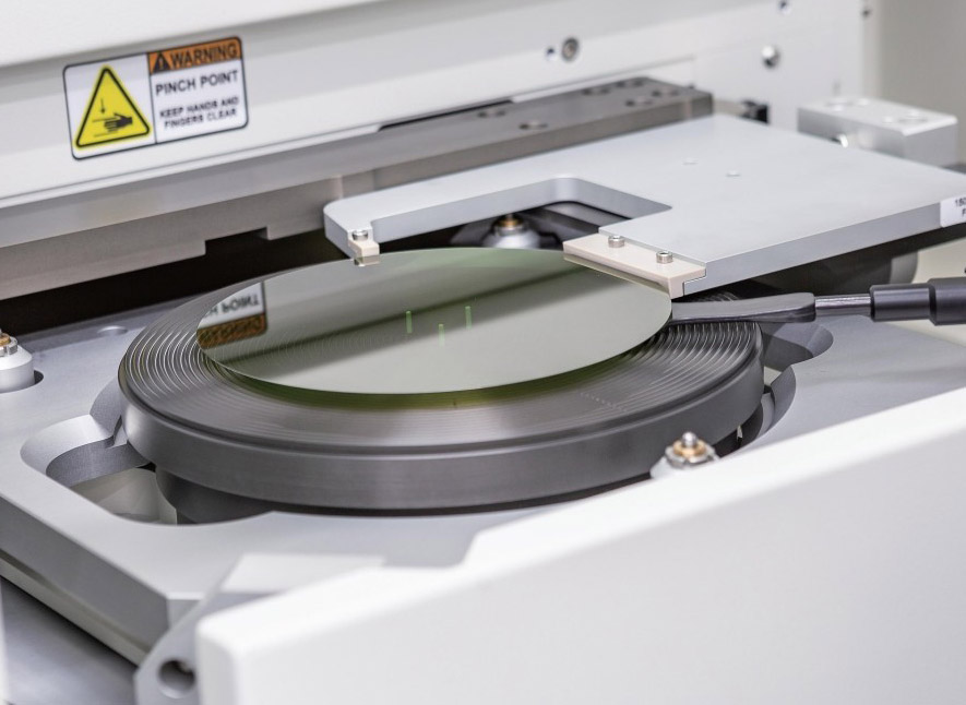
8-inch P-type SiC Wafers
Semicorex 8-inch P-type SiC wafers deliver outstanding performance for next-generation power, RF, and high-temperature devices. Choose Semicorex for superior crystalline quality, industry-leading uniformity, and trusted expertise in advanced SiC materials.*
Send Inquiry
Product Description
Semicorex 8-inch P-type SiC wafers represent a breakthrough in wide bandgap semiconductor technology, offering superior performance for high-power, high-frequency, and high-temperature applications. Manufactured with state-of-the-art crystal growth and wafering processes. In order to realize the functions of various semiconductor devices, the conductivity of semiconductor materials needs to be precisely controlled. P-type doping is one of the important means to change the conductivity of SiC. The introduction of impurity atoms with a small number of valence electrons (usually aluminum) into the SiC lattice will form positively charged "holes". These holes can participate in conduction as carriers, making the SiC material exhibit P-type conductivity. P-type doping is essential for the manufacture of a variety of semiconductor devices, such as MOSFETs, diodes, and bipolar junction transistors, all of which rely on P-N junctions to achieve their specific functions. Aluminum (Al) is a commonly used P-type dopant in SiC. Compared with boron, aluminum is generally more suitable for obtaining heavily doped, low-resistance SiC layers. This is because aluminum has a shallower acceptor energy level and is more likely to occupy the position of silicon atoms in the SiC lattice, thereby achieving higher doping efficiency. The main method for P-type doping SiC wafers is ion implantation, which usually requires annealing at high temperatures above 1500°C to activate the implanted aluminum atoms, allowing them to enter the replacement position of the SiC lattice and play their electrical role. Due to the low diffusion rate of dopants in SiC, ion implantation technology can accurately control the implantation depth and concentration of impurities, which is crucial for manufacturing high-performance devices.
The choice of dopants and the doping process (such as high-temperature annealing after ion implantation) are key factors affecting the electrical properties of SiC devices. The ionization energy and solubility of the dopant directly determine the number of free carriers. The implantation and annealing processes affect the effective binding and electrical activation of the dopant atoms in the lattice. These factors ultimately determine the voltage tolerance, current carrying capacity and switching characteristics of the device. High-temperature annealing is usually required to achieve electrical activation of dopants in SiC, which is an important manufacturing step. Such high annealing temperatures place high demands on equipment and process control, which need to be precisely controlled to avoid introducing defects in the material or reducing the quality of the material. Manufacturers need to optimize the annealing process to ensure sufficient activation of dopants while minimizing adverse effects on wafer integrity.
The high-quality, low-resistance P-type silicon carbide substrate produced by the liquid phase method will greatly accelerate the development of high-performance SiC-IGBT and realize the localization of high-end ultra-high voltage power devices. The liquid phase method has the advantage of growing high-quality crystals. The crystal growth principle determines that ultra-high-quality silicon carbide crystals can be grown, and silicon carbide crystals with low through-dislocations and zero stacking faults have been obtained. The P-type 4-degree off-angle silicon carbide substrate prepared by the liquid phase method has a resistivity of less than 200mΩ·cm, a uniform in-plane resistivity distribution, and good crystallinity.
P-type silicon carbide substrates are generally used to make power devices, such as insulated gate bipolar transistors (IGBT).
IGBT = MOSFET + BJT, which is a switch that is either on or off. MOSFET = IGFET (metal oxide semiconductor field effect transistor, or insulated gate field effect transistor). BJT (Bipolar Junction Transistor, also known as triode), bipolar means that when working, two types of carriers, electrons and holes, participate in the conduction process, generally a PN junction participates in the conduction.
Liquid Phase Method is a valuable technique for producing P-type SiC substrates with controlled doping and high crystal quality. While it faces challenges, its advantages make it suitable for specific applications in high-power electronics. The use of Aluminium as a dopant is the most common way to create the P type SiC.
The push for higher efficiency, higher power density, and greater reliability in power electronics (for electric vehicles, renewable energy inverters, industrial motor drives, power supplies, etc.) necessitates SiC devices that operate closer to the material's theoretical limits. Defects originating from the substrate are a major limiting factor. P-type SiC has historically been more defect-prone than n-type when grown by traditional PVT. Therefore, high-quality, low-defect p-type SiC substrates, enabled by methods like LPM, are critical enablers for the next generation of advanced SiC power devices, particularly MOSFETs and diodes.
Hot Tags: 8-inch P-type SiC Wafers, China, Manufacturers, Suppliers, Factory, Customized, Bulk, Advanced, Durable
Product Tag
Related Category
Send Inquiry
Please feel free to give your inquiry in the form below. We will reply you in 24 hours.


