
- English
- Español
- Português
- русский
- Français
- 日本語
- Deutsch
- tiếng Việt
- Italiano
- Nederlands
- ภาษาไทย
- Polski
- 한국어
- Svenska
- magyar
- Malay
- বাংলা ভাষার
- Dansk
- Suomi
- हिन्दी
- Pilipino
- Türkçe
- Gaeilge
- العربية
- Indonesia
- Norsk
- تمل
- český
- ελληνικά
- український
- Javanese
- فارسی
- தமிழ்
- తెలుగు
- नेपाली
- Burmese
- български
- ລາວ
- Latine
- Қазақша
- Euskal
- Azərbaycan
- Slovenský jazyk
- Македонски
- Lietuvos
- Eesti Keel
- Română
- Slovenski
- मराठी
- Srpski језик
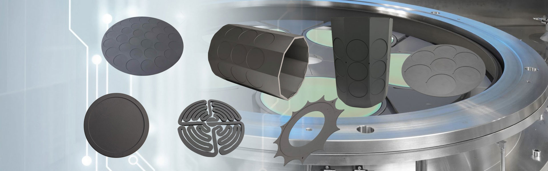


6 Inch Semi-Insulating HPSI SiC Wafer
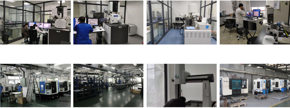
Semicorex provides various types of 4H and 6H SiC wafers. We have been manufacturer and supplier of silicon carbide products for many years. Our double-polished 6 Inch Semi-Insulating HPSI SiC Wafer has a good price advantage and cover most of the European and American markets. We look forward to becoming your long-term partner in China.
Send Inquiry
Product Description
Semicorex has a complete silicon carbide(SiC) wafer products line, including 4H and 6H substrates with N-type, P-type and high purity semi-insulating wafers, they can be with or without epitaxy.
The 6 inch diameter of our 6 Inch Semi-Insulating HPSI SiC Wafer provides a large surface area for manufacturing power electronic devices such as MOSFETs, Schottky diodes, and other high-voltage applications. 6 Inch Semi-Insulating HPSI SiC Wafer is mainly used in 5G communications, radar systems, guidance heads, satellite communications, warplanes and other fields, with the advantages of enhancing the RF range, ultra-long-range identification, anti-jamming and high-speed, high-capacity information transfer applications, is considered the most ideal substrate for making microwave power devices.
Specifications:
● Diameter: 6″
●Double-polished
● Grade: Production, Research, Dummy
● 4H-SiC HPSI Wafer
● Thickness: 500±25 μm
● Micropipe Density: ≤1 ea/cm2 ~ ≤15 ea/cm2
|
Items |
Production |
Research |
Dummy |
|
Crystal Parameters |
|||
|
Polytype |
4H |
||
|
Surface orientation on-axis |
<0001 > |
||
|
Surface orientation off-axis |
0±0.2° |
||
|
(0004)FWHM |
≤45arcsec |
≤60arcsec |
≤1OOarcsec |
|
Electrical Parameters |
|||
|
Type |
HPSI |
||
|
Resistivity |
≥1 E8ohm·cm |
100% area > 1 E5ohm·cm |
70% area > 1 E5ohm·cm |
|
Mechanical Parameters |
|||
|
Diameter |
150±0.2 mm |
||
|
Thickness |
500±25 μm |
||
|
Primary flat orientation |
[1-100]±5° or Notch |
||
|
Primary flat length/depth |
47.5±1.5mm or 1 - 1.25mm |
||
|
TTV |
≤5 μm |
≤10 μm |
≤15 μm |
|
LTV |
≤3 μm(5mm*5mm) |
≤5 μm(5mm*5mm) |
≤10 μm(5mm*5mm) |
|
Bow |
-15μm ~ 15μm |
-35μm ~ 35μm |
-45μm ~ 45μm |
|
Warp |
≤35 μm |
≤45 μm |
≤55 μm |
|
Front(Si-face) roughness(AFM) |
Ra≤0.2nm (5μm*5μm) |
||
|
Structure |
|||
|
Micropipe density |
≤1 ea/cm2 |
≤10 ea/cm2 |
≤15 ea/cm2 |
|
Carbon inclusion density |
≤1 ea/cm2 |
NA |
|
|
Hexagonal void |
None |
NA |
|
|
Metal impurities |
≤5E12atoms/cm2 |
NA |
|
|
Front Quality |
|||
|
Front |
Si |
||
|
Surface finish |
Si-face CMP |
||
|
Particles |
≤60ea/wafer (size≥0.3μm) |
NA |
|
|
Scratches |
≤5ea/mm. Cumulative length ≤Diameter |
Cumulative length≤300mm |
NA |
|
Orange peel/pits/stains/striations/ cracks/contamination |
None |
NA |
|
|
Edge chips/indents/fracture/hex plates |
None |
||
|
Polytype areas |
None |
Cumulative area≤20% |
Cumulative area≤30% |
|
Front laser marking |
None |
||
|
Back Quality |
|||
|
Back finish |
C-face CMP |
||
|
Scratches |
≤5ea/mm,Cumulative length≤2*Diameter |
NA |
|
|
Back defects (edge chips/indents) |
None |
||
|
Back roughness |
Ra≤0.2nm (5μm*5μm) |
||
|
Back laser marking |
"SEMI" |
||
|
Edge |
|||
|
Edge |
Chamfer |
||
|
Packaging |
|||
|
Packaging |
Epi-ready with vacuum packaging Multi-wafer cassette packaging |
||
|
*Notes: "NA" means no request Items not mentioned may refer to SEMI-STD. |
|||

Hot Tags: 6 Inch Semi-Insulating HPSI SiC Wafer, China, Manufacturers, Suppliers, Factory, Customized, Bulk, Advanced, Durable
Related Category
Send Inquiry
Please feel free to give your inquiry in the form below. We will reply you in 24 hours.


