
- English
- Español
- Português
- русский
- Français
- 日本語
- Deutsch
- tiếng Việt
- Italiano
- Nederlands
- ภาษาไทย
- Polski
- 한국어
- Svenska
- magyar
- Malay
- বাংলা ভাষার
- Dansk
- Suomi
- हिन्दी
- Pilipino
- Türkçe
- Gaeilge
- العربية
- Indonesia
- Norsk
- تمل
- český
- ελληνικά
- український
- Javanese
- فارسی
- தமிழ்
- తెలుగు
- नेपाली
- Burmese
- български
- ລາວ
- Latine
- Қазақша
- Euskal
- Azərbaycan
- Slovenský jazyk
- Македонски
- Lietuvos
- Eesti Keel
- Română
- Slovenski
- मराठी
- Srpski језик


12-inch Semi-Insulating SiC Substrates
Semicorex 12-inch Semi-Insulating SiC Substrates are next-generation material designed for high-frequency, high-power, and high-reliability semiconductor applications. Choosing Semicorex means partnering with a trusted leader in SiC innovation, committed to delivering exceptional quality, precision engineering, and customized solutions to empower your most advanced device technologies.*
Send Inquiry
Product Description
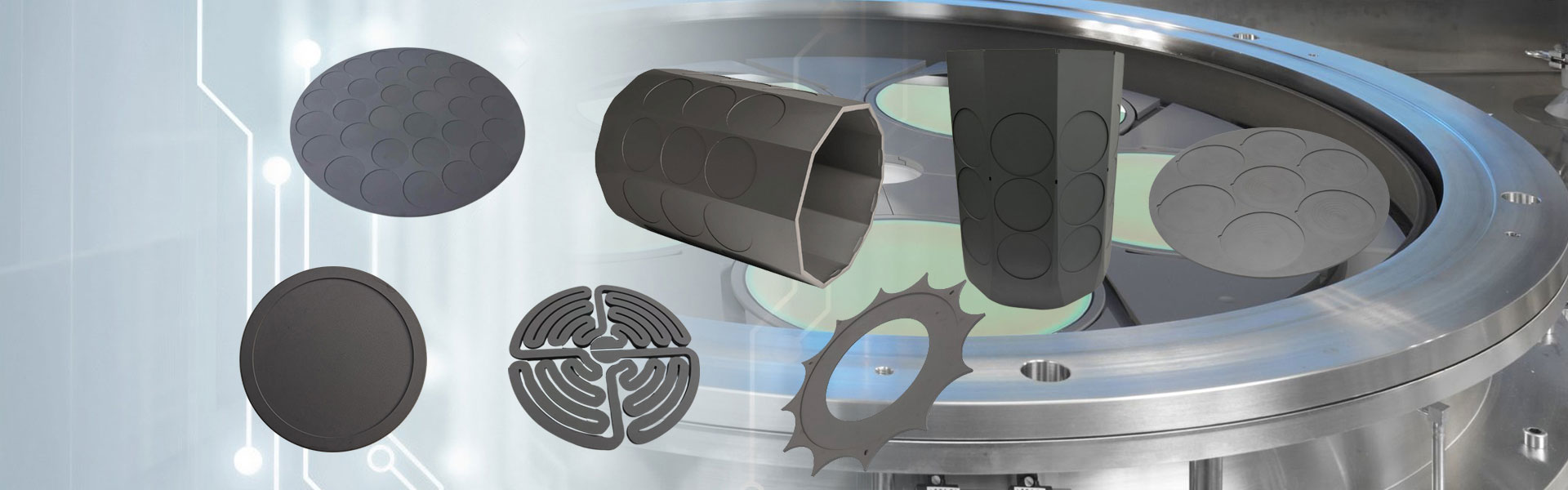
Semicorex 12-inch Semi-Insulating SiC substrates represent a breakthrough in next-generation semiconductor materials, offering unmatched performance for high-frequency, high-power, and radiation-resistant applications. Designed for advanced RF, microwave, and power device fabrication, these large-diameter SiC substrates enable superior device efficiency, reliability, and scalability.
Our 12-inch Semi-Insulating SiC substrates are engineered using advanced growth and processing technologies to achieve high purity and minimal defect density. With a resistivity typically greater than 10⁹ Ω·cm, they effectively suppress parasitic conduction, ensuring optimal device isolation. The material exhibits outstanding thermal conductivity (> 4.5 W/cm·K), superior chemical stability, and high breakdown electric field strength, making it ideal for demanding environments and cutting-edge device architectures.

Silicon carbide (SiC) is a compound semiconductor material composed of carbon and silicon. It is one of the ideal materials for making high-temperature, high-frequency, high-power, and high-voltage devices. Compared with traditional silicon materials (Si), the bandgap width of silicon carbide is 3 times that of silicon; the thermal conductivity is 4-5 times that of silicon; the breakdown voltage is 8-10 times that of silicon; the electron saturation drift rate is 2-3 times that of silicon, which meets the needs of modern industry for high power, high voltage, and high frequency. It is mainly used to make high-speed, high-frequency, high-power and light-emitting electronic components. Downstream application areas include smart grids, new energy vehicles, photovoltaic wind power, 5G communications, etc. In the field of power devices, silicon carbide diodes and MOSFETs have begun commercial applications.
The silicon carbide industry chain mainly includes substrates, epitaxy, device design, manufacturing, packaging and testing. From materials to semiconductor power devices, silicon carbide will go through single crystal growth, ingot slicing, epitaxial growth, wafer design, manufacturing, packaging and other process flows. After synthesizing silicon carbide powder, silicon carbide ingots are first made, and then silicon carbide substrates are obtained through slicing, grinding and polishing, and epitaxial growth is performed to obtain epitaxial wafers. The epitaxial wafers are subjected to processes such as photolithography, etching, ion implantation, and metal passivation to obtain silicon carbide wafers, which are cut into dies and packaged to obtain devices. The devices are combined and put into a special housing to assemble into modules.
From the perspective of electrochemical properties, silicon carbide substrate materials can be divided into conductive substrates (resistivity range 15~30mΩ·cm) and semi-insulating substrates (resistivity higher than 105Ω·cm). These two types of substrates are used to manufacture discrete devices such as power devices and radio frequency devices after epitaxial growth. Among them, 12-inch Semi-Insulating SiC substrates are mainly used to manufacture gallium nitride radio frequency devices, optoelectronic devices, etc. By growing a gallium nitride epitaxial layer on a semi-insulating silicon carbide substrate, a silicon carbide-based gallium nitride epitaxial wafer is obtained, which can be further made into gallium nitride radio frequency devices such as HEMT. Conductive silicon carbide substrates are mainly used to manufacture power devices. Unlike the traditional silicon power device manufacturing process, silicon carbide power devices cannot be directly manufactured on a silicon carbide substrate. It is necessary to grow a silicon carbide epitaxial layer on a conductive substrate to obtain a silicon carbide epitaxial wafer, and then manufacture Schottky diodes, MOSFETs, IGBTs and other power devices on the epitaxial layer.
Hot Tags: 12-inch Semi-Insulating SiC Substrates, China, Manufacturers, Suppliers, Factory, Customized, Bulk, Advanced, Durable
Product Tag
Related Category
Send Inquiry
Please feel free to give your inquiry in the form below. We will reply you in 24 hours.


