- English
- Español
- Português
- русский
- Français
- 日本語
- Deutsch
- tiếng Việt
- Italiano
- Nederlands
- ภาษาไทย
- Polski
- 한국어
- Svenska
- magyar
- Malay
- বাংলা ভাষার
- Dansk
- Suomi
- हिन्दी
- Pilipino
- Türkçe
- Gaeilge
- العربية
- Indonesia
- Norsk
- تمل
- český
- ελληνικά
- український
- Javanese
- فارسی
- தமிழ்
- తెలుగు
- नेपाली
- Burmese
- български
- ລາວ
- Latine
- Қазақша
- Euskal
- Azərbaycan
- Slovenský jazyk
- Македонски
- Lietuvos
- Eesti Keel
- Română
- Slovenski
- मराठी
- Srpski језик
Industry News
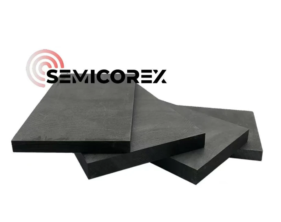
Brief Introduction of High-Purity Graphite Plates
High-purity graphite plates are the plate-shaped carbon materials made from premium raw materials including petroleum coke, pitch coke or high-purity natural graphite through a series of production processes like calcination, kneading, forming, baking, high-temperature graphitization (above 2800℃) a......
Read MoreNew Research Findings On Graphene
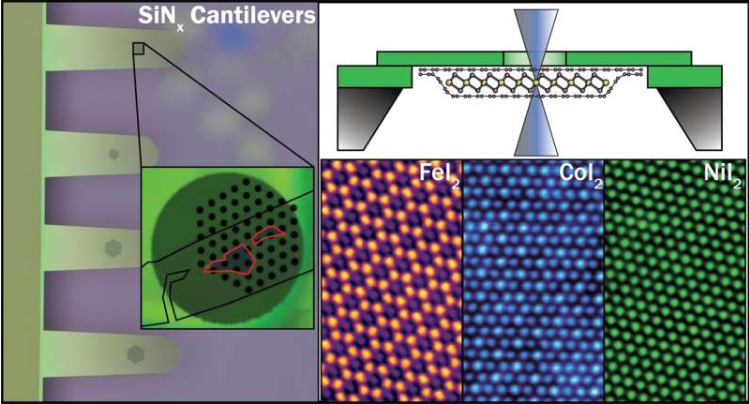
Two-dimensional materials promise revolutionary advancements in electronics and photonics, but many of the most promising candidates degrade within seconds of exposure to air, making them virtually unsuitable for research or integration into practical technologies. Transition metal dihalides are a h......
Read MoreWhat are the LPCVD Processes?
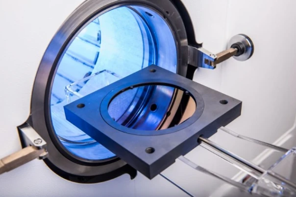
ow pressure chemical vapor deposition (LPCVD) processes are the CVD techniques that deposit thin film materials on wafer surfaces under low pressure environments. LPCVD processes are widely used in material deposition technologies for semiconductor manufacturing, optoelectronics, and thin-film solar......
Read MoreTantalum Carbide Ceramics – A Key Material in Semiconductor and Aerospace.
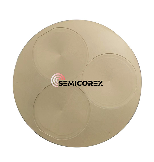
Tantalum carbide (TaC) is an ultra-high temperature ceramic material. Ultra-high temperature ceramics (UHTCs) generally refer to ceramic materials with melting points exceeding 3000℃ and used in high-temperature and corrosive environments (such as oxygen atom environments) above 2000℃, such as ZrC, ......
Read MoreMarket development of carbon ceramic materials
Carbon-ceramic composites have seen one of the fastest-growing areas of demand in the high-end equipment manufacturing sector in recent years. Essentially, carbon-ceramic composites introduce a silicon silicide ceramic phase into a carbon fiber-reinforced carbon matrix, constructing a multiphase com......
Read MoreWhat Are the Carbon-Ceramic Composites?
As the rising demand in the field of cutting-edge equipment manufacturing, carbon-ceramic composites are increasingly regarded as the promising materials for next-generation of high-performance friction systems and high-temperature structural components. So what are the carbon-ceramic composites? Fu......
Read More
