
- English
- Español
- Português
- русский
- Français
- 日本語
- Deutsch
- tiếng Việt
- Italiano
- Nederlands
- ภาษาไทย
- Polski
- 한국어
- Svenska
- magyar
- Malay
- বাংলা ভাষার
- Dansk
- Suomi
- हिन्दी
- Pilipino
- Türkçe
- Gaeilge
- العربية
- Indonesia
- Norsk
- تمل
- český
- ελληνικά
- український
- Javanese
- فارسی
- தமிழ்
- తెలుగు
- नेपाली
- Burmese
- български
- ລາວ
- Latine
- Қазақша
- Euskal
- Azərbaycan
- Slovenský jazyk
- Македонски
- Lietuvos
- Eesti Keel
- Română
- Slovenski
- मराठी
- Srpski језик

What is the particle defects?
Particle defects refer to the tiny particulate inclusions inside or on the semiconductor wafers. They can damage the structural integrity of semiconductor devices and cause electrical faults such as short circuits and open circuits. Since these problems caused by particle defects can seriously affect the long-term reliability of semiconductor devices, particle defects must be strictly controlled in semiconductor manufacturing.
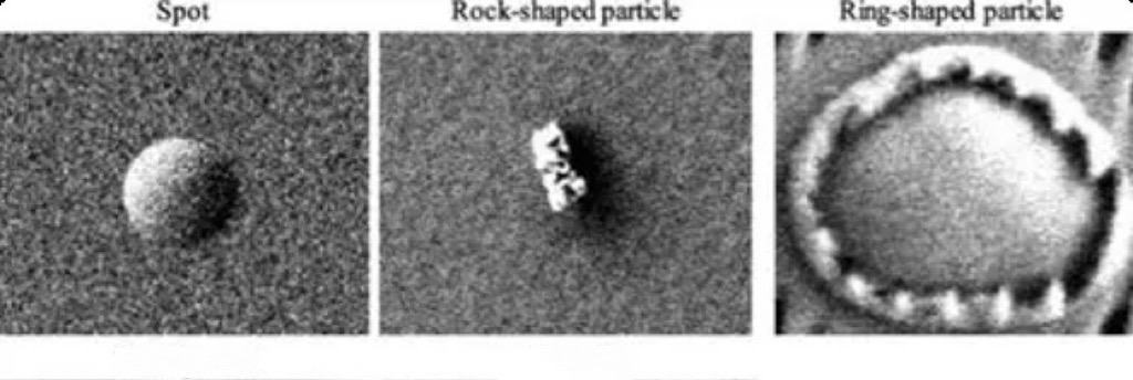
According to their positions and characteristics, particle defects can be divided into two major categories: surface particles and in-film particles. Surface particles refer to the particles that fall on the wafer surface in the process environment, usually presenting as clusters with sharp corners. In-film particles refer to those that fall into the wafer during the film formation process and are covered by subsequent films, with defects embedded within the film layer.
How are particle defects generated?
The generation of particle defects is caused by multiple factors. During the wafer manufacturing process, thermal stress caused by temperature changes and mechanical stress resulting from the handling, processing and heat treatment of wafers can lead to surface cracks or material shedding on wafers, which is one of the main reasons for particle defects. Chemical corrosion caused by reaction reagents and reaction gases is another main cause of particle defects. During the corrosion process, unwanted products or impurities are produced and adhere to the wafer surface to form particle defects. In addition to the two main factors mentioned above, impurities in raw materials, internal contamination of equipment, environmental dust and operational errors are also common reasons of particle defects.
How to detect and control particle defects?
The detection of particle defects mainly relies on high-precision microscopy technology. Scanning electron microscopy (SEM) has become a core tool for defect detection due to its high resolution and imaging capabilities, capable of revealing the morphology, size and distribution of tiny particles. Atomic force microscopy (AFM) maps three-dimensional surface topography by detecting interatomic forces and has extremely high precision in nanoscale defect detection. Optical microscopes are used for rapid screening of larger defects.
To control particle defects, multiple measures need to be taken.
1.Precisely control parameters such as etching rate, deposition thickness, temperature and pressure.
2.Use high-purity raw materials for semiconductor wafer fabrication.
3.Adopt high-precision and high-stability equipment and carry out regular maintenance and cleaning.
4.Enhance operator skills through specialized training, standardize operational practices, and strengthen process monitoring and management.
It is necessary to comprehensively analyze the causes of particle defects, identify the contamination points and take targeted solutions to effectively reduce the incidence of particle defects.


