
- English
- Español
- Português
- русский
- Français
- 日本語
- Deutsch
- tiếng Việt
- Italiano
- Nederlands
- ภาษาไทย
- Polski
- 한국어
- Svenska
- magyar
- Malay
- বাংলা ভাষার
- Dansk
- Suomi
- हिन्दी
- Pilipino
- Türkçe
- Gaeilge
- العربية
- Indonesia
- Norsk
- تمل
- český
- ελληνικά
- український
- Javanese
- فارسی
- தமிழ்
- తెలుగు
- नेपाली
- Burmese
- български
- ລາວ
- Latine
- Қазақша
- Euskal
- Azərbaycan
- Slovenský jazyk
- Македонски
- Lietuvos
- Eesti Keel
- Română
- Slovenski
- मराठी
- Srpski језик
Industry News
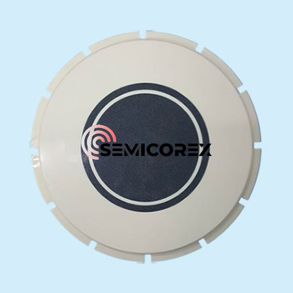
Why Is a Customized Porous Ceramic Chuck the Ultimate Solution for High-Precision Semiconductor Manufacturing
As semiconductor devices become smaller, thinner, and more complex, wafer handling technologies must achieve unprecedented levels of precision and stability. A Customized Porous Ceramic Chuck has emerged as a critical component in advanced semiconductor manufacturing, offering uniform vacuum adsorpt......
Read More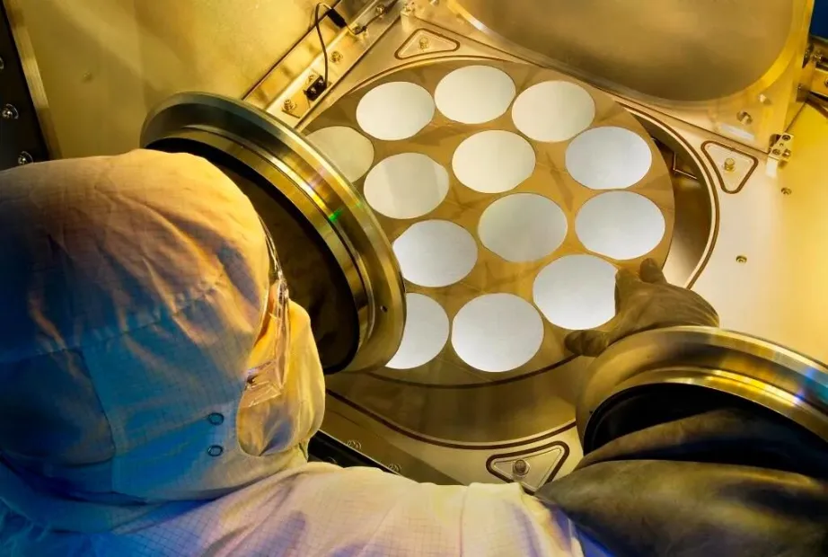
Why Are CVD SiC Coatings a Must for MOCVD Graphite Susceptors?
In LED chip manufacturing, MOCVD epitaxy serves as the core process that determines luminous efficiency. During production, graphite susceptors carrying sapphire or silicon substrates operate under repeated thermal cycles at temperatures close to 1,000°C within corrosive atmospheres. Accordingly, th......
Read More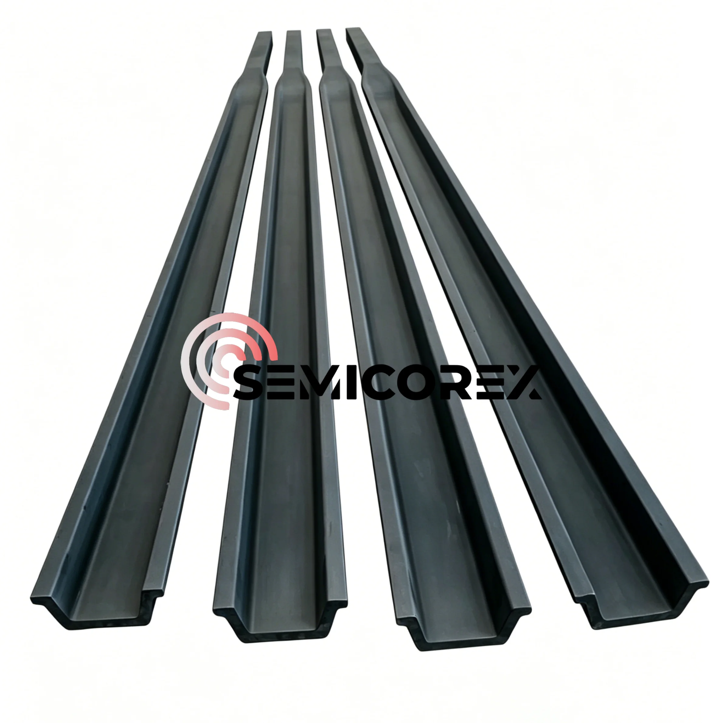
Are Silicon Carbide Cantilever Paddles the Ultimate Solution for High-Temperature Semiconductor Processing
As semiconductor manufacturing continues to evolve toward larger wafer sizes, higher processing temperatures, and stricter contamination control requirements, Silicon Carbide Cantilever Paddles have become an essential component in advanced thermal processing systems. Semicorex specializes in high-p......
Read More
Core Applications of Alumina Ceramic Components in the Semiconductor
As a leading advanced ceramic for semiconductor applications, alumina ceramics strike an optimal balance between cost, machinability and overall performance. Featuring high hardness, excellent insulation, outstanding corrosion resistance and low thermal expansion, they fully meet the stringent requi......
Read More
NVIDIA Rubin GPUs Fully Switch to Graphene Thermal Pads
In May 2026, NVIDIA finalized its decision to completely abandon liquid metal in the standard Vera Rubin (1800-2000W TDP) and switch to high thermal conductivity graphene pads for mass production; the Ultra high-end version (2500-2850W) will retain the extreme solution of liquid metal + microchann......
Read More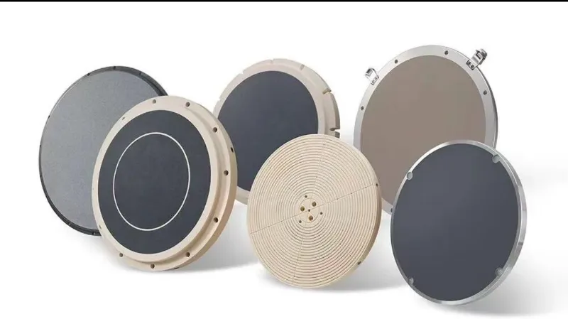
Why Are Porous Alumina Chucks Becoming the Preferred Choice for Precision Semiconductor Manufacturing
The semiconductor industry continues to demand higher precision, cleaner processing environments, and greater manufacturing efficiency. As wafer sizes increase and process tolerances become increasingly stringent, traditional wafer holding methods often struggle to meet modern production requirement......
Read More