- English
- Español
- Português
- русский
- Français
- 日本語
- Deutsch
- tiếng Việt
- Italiano
- Nederlands
- ภาษาไทย
- Polski
- 한국어
- Svenska
- magyar
- Malay
- বাংলা ভাষার
- Dansk
- Suomi
- हिन्दी
- Pilipino
- Türkçe
- Gaeilge
- العربية
- Indonesia
- Norsk
- تمل
- český
- ελληνικά
- український
- Javanese
- فارسی
- தமிழ்
- తెలుగు
- नेपाली
- Burmese
- български
- ລາວ
- Latine
- Қазақша
- Euskal
- Azərbaycan
- Slovenský jazyk
- Македонски
- Lietuvos
- Eesti Keel
- Română
- Slovenski
- मराठी
- Srpski језик
What is The Semiconductor Wafer Cleaning?
Wafer cleaning refers to the process of removing particulate contaminants, organic contaminants, metal contaminants, and natural oxide layers from the wafer surface using physical or chemical methods before semiconductor processes such as oxidation, photolithography, epitaxy, diffusion, and wire evaporation. In the semiconductor manufacturing, the yield rate of semiconductor devices largely depends on the cleanliness of the semiconductor wafer surface. Therefore, to achieve the cleanliness required for semiconductor manufacturing, the rigorous wafer cleaning processes are essential.
Mainstream technologies for wafer cleaning
1.Dry cleaning: plasma cleaning technology, vapor phase cleaning technology.
2.Wet chemical cleaning: Solution immersion method, mechanical scrubbing method, ultrasonic cleaning technology, megasonic cleaning technology, rotary spray method.
3.Beam cleaning: Micro-beam cleaning technology, laser beam technology, condensation spray technology.
The classification of contaminants originate from various sources, and are commonly classified into the following four categories according to their properties:
1.Particulate contaminants
Particulate contaminants mainly consists of polymers, photoresists, and etching impurities. These contaminants usually adheres to the surface of semiconductor wafers, which may cause problems like photolithography defects, etching blockage, thin-film pinholes, and short circuits. Their adhesion force is mainly van der Waals attraction, which can be eliminated by breaking the electrostatic adsorption between the particles and the wafer surface using physical forces (such as ultrasonic cavitation) or chemical solutions (such as SC-1).
2.Organic contaminants
Organic contaminants mainly come from human skin oils, cleanroom air, machine oil, silicone vacuum grease, photoresist, and cleaning solvents. They may change the surface hydrophobicity, increase the surface roughness and cause surface fogging of semiconductor wafers, thus affecting epitaxial layer growth and thin film deposition uniformity. For this reason, cleaning organic contaminants is usually conducted as the first step of the overall wafer cleaning sequence, where strong oxidants (e.g., sulfuric acid/hydrogen peroxide mixture, SPM) are used to decompose and remove organic contaminants effectively.
3.Metal contaminants
In semiconductor manufacturing processes, metal contaminants (such as Na, Fe, Ni, Cu, Zn, etc.) originating from process chemicals, equipment component wear, and environmental dust adheres to the wafer surface in atomic, ionic, or particulate form. They may lead to problems like leakage current, threshold voltage drift, and shortened carrier lifetime in semiconductor devices, severely impacting chip performance and yield. These type of metal contaminants can be effectively removed using a mixture of hydrochloric acid or hydrogen peroxide (SC-2).
4.Natural oxide layers
Natural oxide layers on wafer surface may impede metal deposition, leading to increased contact resistance, affecting etching uniformity and depth control, and interfering with the doping distribution of ion implantation. HF etching (DHF or BHF) is commonly adopted for oxide removal to secure interfacial integrity in subsequent processes.
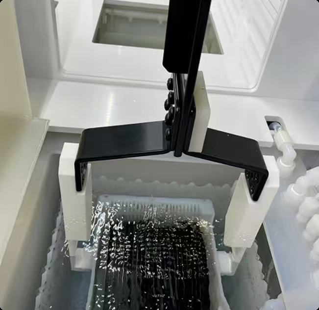
Semicorex offers high-quality quartz cleaning tanks for chemical wet cleaning. If you have any inquiries or need additional details, please don't hesitate to get in touch with us.
Contact phone # +86-13567891907
Email: sales@semicorex.com


