
- English
- Español
- Português
- русский
- Français
- 日本語
- Deutsch
- tiếng Việt
- Italiano
- Nederlands
- ภาษาไทย
- Polski
- 한국어
- Svenska
- magyar
- Malay
- বাংলা ভাষার
- Dansk
- Suomi
- हिन्दी
- Pilipino
- Türkçe
- Gaeilge
- العربية
- Indonesia
- Norsk
- تمل
- český
- ελληνικά
- український
- Javanese
- فارسی
- தமிழ்
- తెలుగు
- नेपाली
- Burmese
- български
- ລາວ
- Latine
- Қазақша
- Euskal
- Azərbaycan
- Slovenský jazyk
- Македонски
- Lietuvos
- Eesti Keel
- Română
- Slovenski
- मराठी
- Srpski језик
Industry News
Semiconductor etching process technology
Etching, or etching, is a crucial step in semiconductor manufacturing, microelectronics IC manufacturing, and micro/nano manufacturing processes. It's a primary patterning process associated with photolithography. In a narrow sense, etching is essentially photolithographic etching, where photoresist......
Read More
Reasons for the Gap Between Practical and Theoretical Thermal Conductivity of Silicon Nitride Ceramics
Silicon nitride (Si₃N₄) is a structural ceramic material with the intrinsic thermal conductivity around 320 W/(m·K), featuring high thermal conductivity and outstanding mechanical properties. Thanks to its superior stability at ambient temperature, Si₃N₄ has become a widely adopted ceramic substrate......
Read More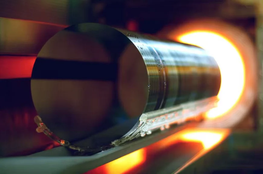
Main Types of Thermal Oxidation
In high-end semiconductor device fabrication, SiO₂ films are typically formed via oxidation processes for substrate surface treatment, and their common applications include dopant barrier layers, surface insulation layers, gate oxide layers, field oxides and sacrificial oxides. As the core processes......
Read More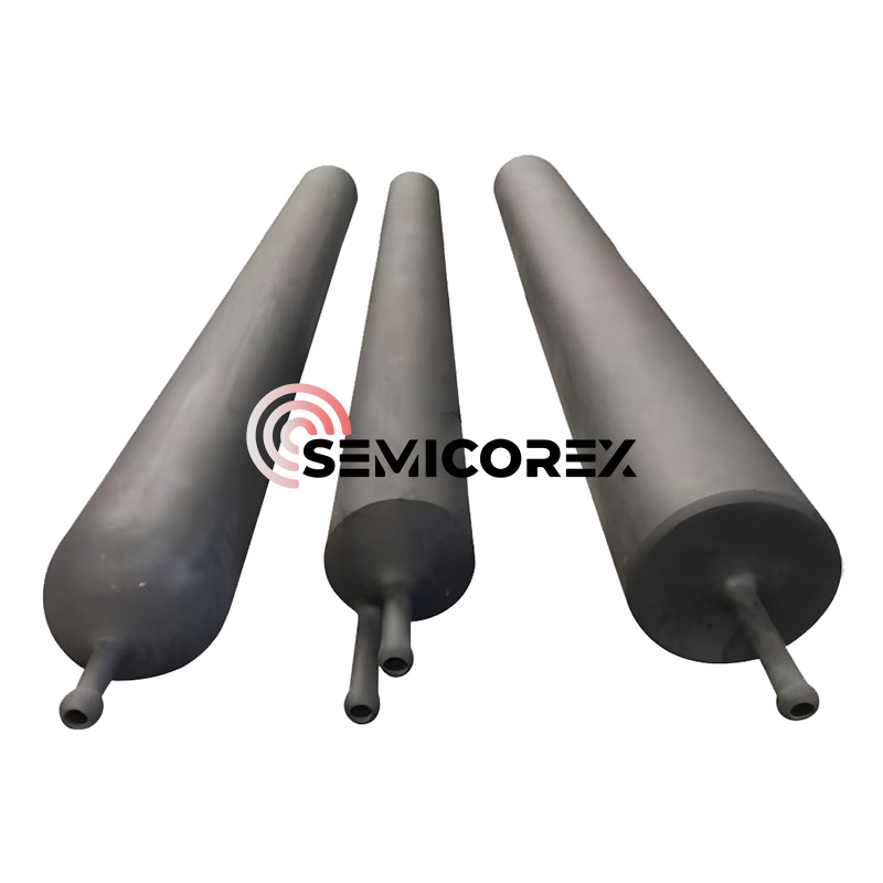
Semicorex Ceramic applied in Semiconductor processing
With the advancement of technology, smart products such as mobile phones, computers, electric vehicles, and robots have become integrated into people's lives. These products contain a large number of semiconductor chips, and chip fabrication requires semiconductor equipment, such as etching machines......
Read More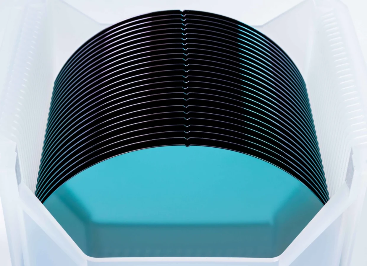
Brief Introduction to High-Resistivity Silicon Wafers
High-resistivity silicon wafers (HR-Si), as its name suggests, is a monocrystalline silicon material with extremely high resistivity. In the advanced semiconductor manufacturing field, high-frequency loss has become a major challenge in high-end chip design. Thanks to its ultra-high resistivity, the......
Read More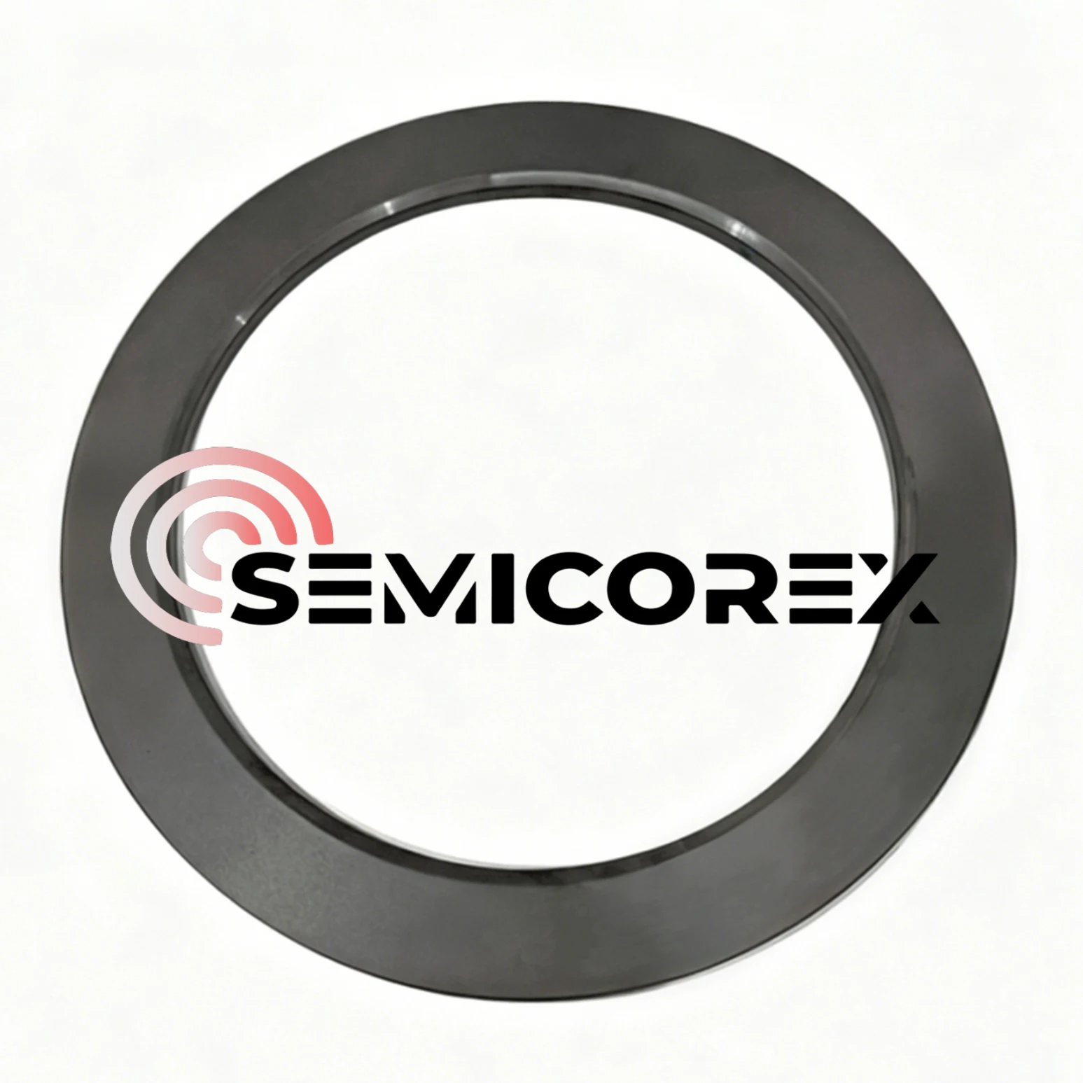
Why Focus Ring Is Indispensable for Etching Equipment?
Focus ring, also referred to as compensation ring or confinement ring, is an indispensable component of etching equipment, especially plasma dry etch equipment. Nanoscale precision etching processes in modern semiconductor manufacturing would not be achievable without it. The use of focus ring ensur......
Read More