
- English
- Español
- Português
- русский
- Français
- 日本語
- Deutsch
- tiếng Việt
- Italiano
- Nederlands
- ภาษาไทย
- Polski
- 한국어
- Svenska
- magyar
- Malay
- বাংলা ভাষার
- Dansk
- Suomi
- हिन्दी
- Pilipino
- Türkçe
- Gaeilge
- العربية
- Indonesia
- Norsk
- تمل
- český
- ελληνικά
- український
- Javanese
- فارسی
- தமிழ்
- తెలుగు
- नेपाली
- Burmese
- български
- ລາວ
- Latine
- Қазақша
- Euskal
- Azərbaycan
- Slovenský jazyk
- Македонски
- Lietuvos
- Eesti Keel
- Română
- Slovenski
- मराठी
- Srpski језик

Etching and Etched Morphology
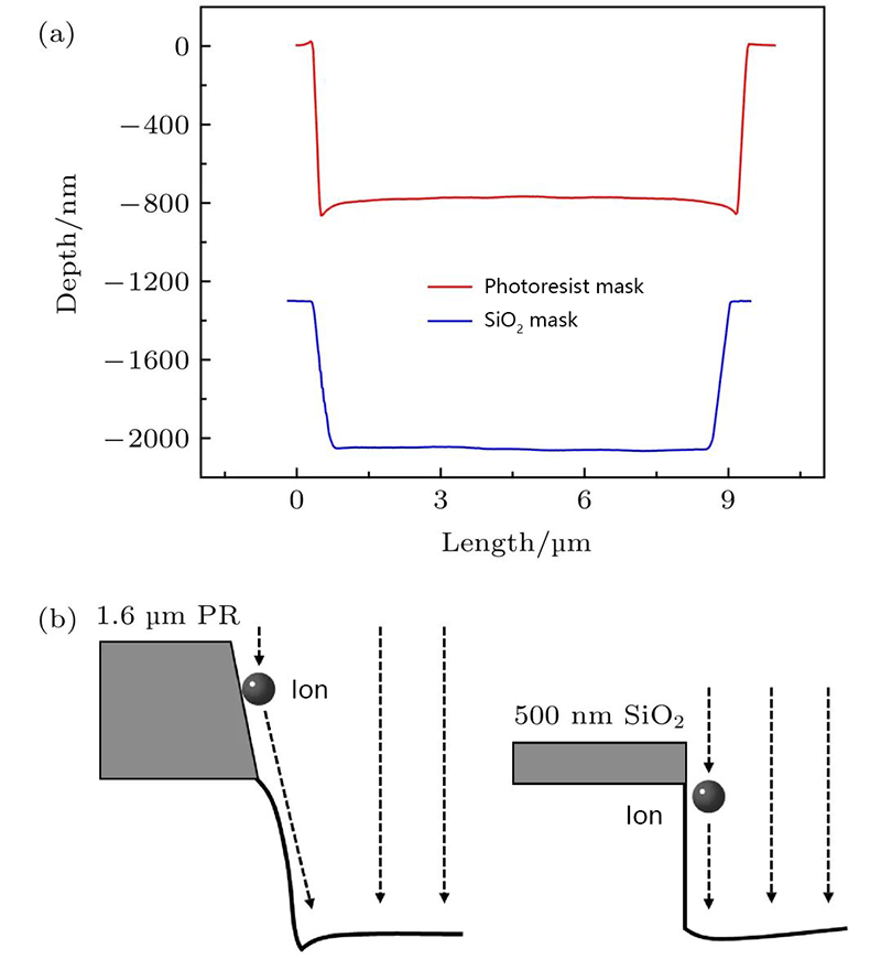
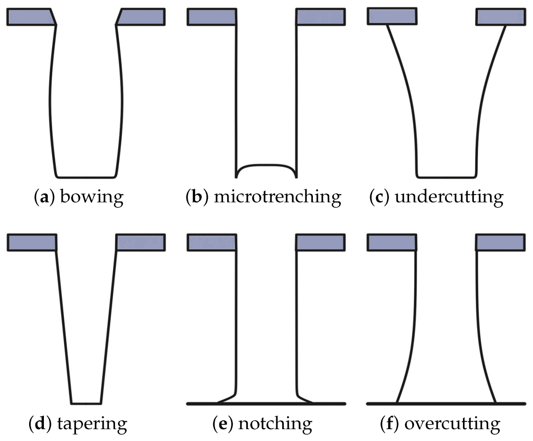
In the semiconductor chip manufacturing process, we are like building a skyscraper on a grain of rice. The lithography machine is like a city planner, using "light" to draw the blueprint for the building on the wafer; while etching is like a sculptor with precision tools, responsible for accurately carving out the channels, holes, and lines according to the blueprint. If you carefully observe the cross-section of these "channels," you'll find that their shapes are not uniform; some are trapezoidal (wider at the top and narrower at the bottom), while others are perfect rectangles (vertical sidewalls). These shapes are not arbitrary; behind them lies a complex interplay of physical and chemical principles, directly determining the chip's performance.
I. Basic Principles of Etching: A Combination of Physical and Chemical Effects
Etching, simply put, is the selective removal of material not protected by photoresist. It is mainly divided into two categories:
1. Wet Etching: Uses chemical solvents (such as acids and alkalis) for etching. It is essentially a purely chemical reaction, and the etching direction is isotropic—that is, it proceeds at the same rate in all directions (front, back, left, right, up, down).
2. Dry Etching (Plasma Etching): This is the mainstream technology today. In a vacuum chamber, process gases (such as gases containing fluorine or chlorine) are introduced, and plasma is generated by a radio frequency power supply. The plasma contains high-energy ions and active free radicals, which work together on the etched surface.
Dry etching can create various shapes precisely because it can flexibly combine the "physical attack" and "chemical attack":
Chemical Composition: Responsible for active free radicals. They react chemically with the wafer surface material, generating volatile products that are then removed. This attack is isotropic, allowing it to "squeeze through" and etch laterally, easily forming trapezoidal shapes.
Physical composition: Positively charged high-energy ions, accelerated by an electric field, bombard the wafer surface perpendicularly. Similar to sandblasting a surface, this "ion bombardment" is anisotropic, primarily vertically downwards, and can "straight-line" carve out the sidewalls.
II. Deciphering Two Classic Profiles: The Birth of Trapezoids and Rectangular Profiles
1. Trapezoid (Tapered Profile) – Primarily Chemical Attack
Formation Principle: When chemical etching dominates the process, while physical bombardment is weaker, the following occurs: etching not only proceeds downwards but also laterally corrodes the area beneath the photoresist mask and exposed sidewalls. This causes the material beneath the protected mask to be gradually "hollowed out," forming a sloping sidewall that is wider at the top and narrower at the bottom, i.e., a trapezoid.
Good Step Coverage: In subsequent thin film deposition processes, the sloping structure of the trapezoid makes it easier for materials (such as metals) to be evenly covered, avoiding fractures at steep corners.
Reduced Stress: The sloping structure better disperses stress, improving device reliability.
High Process Tolerance: Relatively easy to implement.
2. Rectangular (Vertical Profile) – Primarily Physical Attack
Formation Principle: When physical ion bombardment dominates the process, and the chemical composition is carefully controlled, a rectangular profile is formed. High-energy ions, like countless tiny projectiles, bombard the wafer surface almost vertically, achieving extremely high vertical etching rates. Simultaneously, ion bombardment forms a "passivation layer" (e.g., formed by etching byproducts) on the sidewalls; this protective film effectively resists lateral corrosion from chemical free radicals. Ultimately, etching can only proceed vertically downwards, carving out a rectangular structure with nearly 90-degree sidewalls.
In advanced manufacturing processes, transistor density is extremely high, and space is extremely precious.
Highest fidelity: It maintains maximum consistency with the photolithographic blueprint, ensuring accurate critical dimensions (CD) of the device.
Saves area: Vertical structures allow devices to be manufactured in a minimal footprint, key to chip miniaturization.
Semicorex offers precision CVD SiC components in etching. If you have any inquiries or need additional details, please don't hesitate to get in touch with us.
Contact phone # +86-13567891907
Email: sales@semicorex.com


