- English
- Español
- Português
- русский
- Français
- 日本語
- Deutsch
- tiếng Việt
- Italiano
- Nederlands
- ภาษาไทย
- Polski
- 한국어
- Svenska
- magyar
- Malay
- বাংলা ভাষার
- Dansk
- Suomi
- हिन्दी
- Pilipino
- Türkçe
- Gaeilge
- العربية
- Indonesia
- Norsk
- تمل
- český
- ελληνικά
- український
- Javanese
- فارسی
- தமிழ்
- తెలుగు
- नेपाली
- Burmese
- български
- ລາວ
- Latine
- Қазақша
- Euskal
- Azərbaycan
- Slovenský jazyk
- Македонски
- Lietuvos
- Eesti Keel
- Română
- Slovenski
- मराठी
- Srpski језик
Industry News
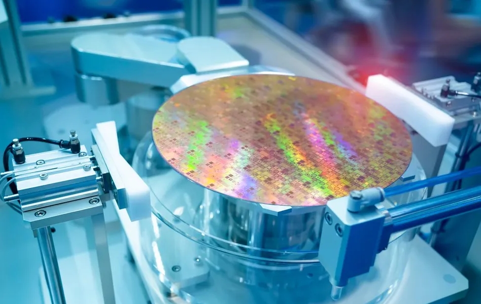
Silicon, Silicon Carbide and Gallium Nitride
Behind the common used digital products and high-tech electric vehicles, 5G base station, there are 3 core semiconductor materials: Silicon, Silicon Carbide and Gallium Nitride driving the industry. They are not alternative for each other, they are the experts in a team, and have the irreplaceable e......
Read More
What is the notch on wafers?
The wafer notch is a V-shaped or U-shaped groove on the edge of a semiconductor wafer. Far from being a defect incurred during the manufacturing process, it is the critical structural marker that was intentionally designed, whose core function lies in enabling precise positioning and orientation ide......
Read More
How Does TaC Coating Protect Graphite Components In Semiconductors
That's where the game-changing innovation of TaC Coating enters the picture, and why our advanced solutions at Semicorex are engineered to directly address your most persistent production pain points. Graphite is fantastic for its thermal properties, but without a robust shield, it simply cannot wit......
Read More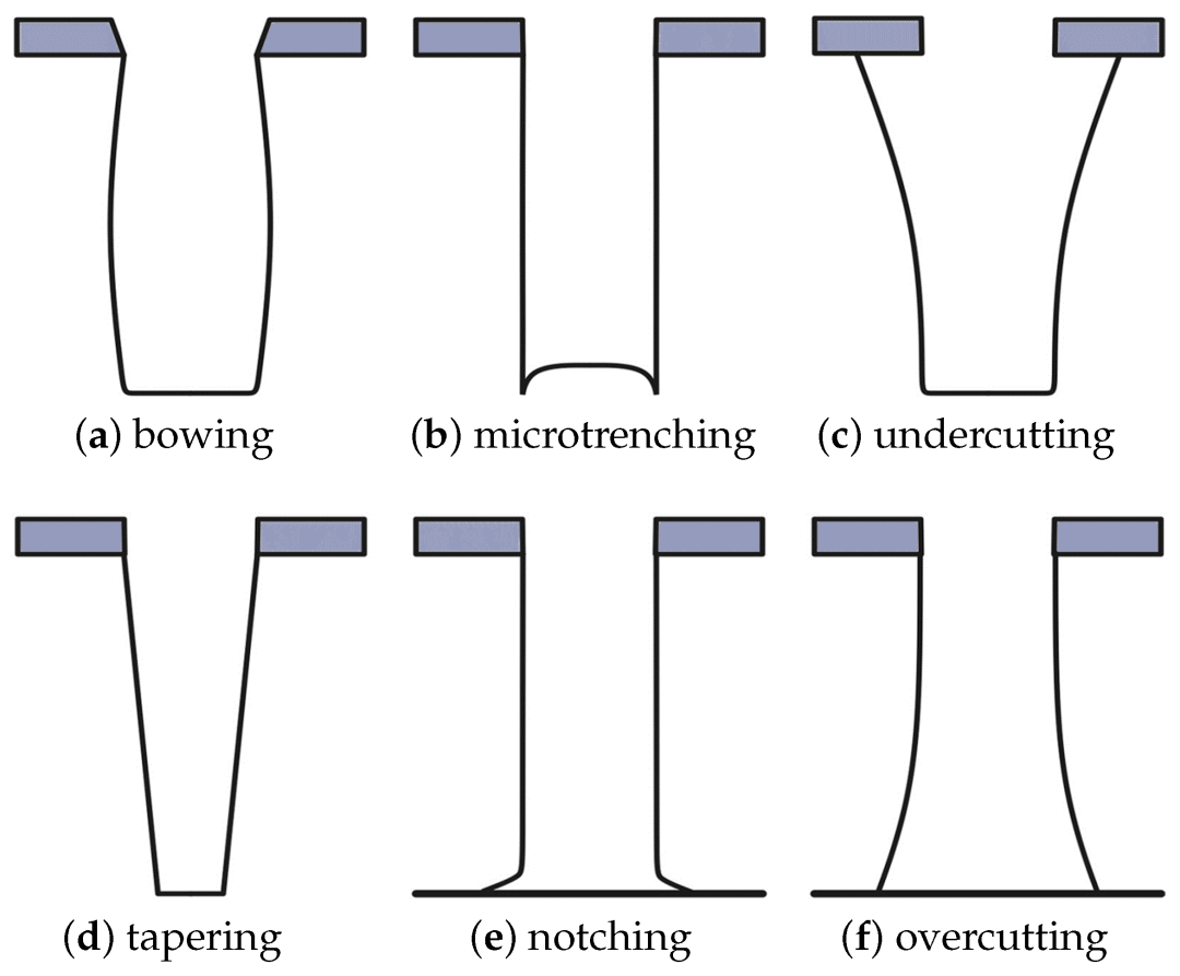
Etching and Etched Morphology
In the semiconductor chip manufacturing process, we are like building a skyscraper on a grain of rice. The lithography machine is like a city planner, using "light" to draw the blueprint for the building on the wafer; while etching is like a sculptor with precision tools, responsible for accurately ......
Read More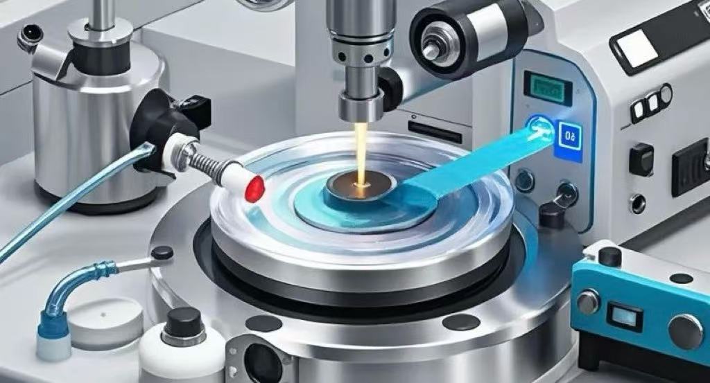
What are dishing and erosion in the CMP process?
Chemical mechanical polishing (CMP), which combines chemical corrosion and mechanical polishing to remove surface imperfections, is the significant semiconductor process for achieving overall planarization of the wafer surface. CMP results in two surface defects, dishing and erosion, which significa......
Read More