- English
- Español
- Português
- русский
- Français
- 日本語
- Deutsch
- tiếng Việt
- Italiano
- Nederlands
- ภาษาไทย
- Polski
- 한국어
- Svenska
- magyar
- Malay
- বাংলা ভাষার
- Dansk
- Suomi
- हिन्दी
- Pilipino
- Türkçe
- Gaeilge
- العربية
- Indonesia
- Norsk
- تمل
- český
- ελληνικά
- український
- Javanese
- فارسی
- தமிழ்
- తెలుగు
- नेपाली
- Burmese
- български
- ລາວ
- Latine
- Қазақша
- Euskal
- Azərbaycan
- Slovenský jazyk
- Македонски
- Lietuvos
- Eesti Keel
- Română
- Slovenski
- मराठी
- Srpski језик
Silicon Shield Ring
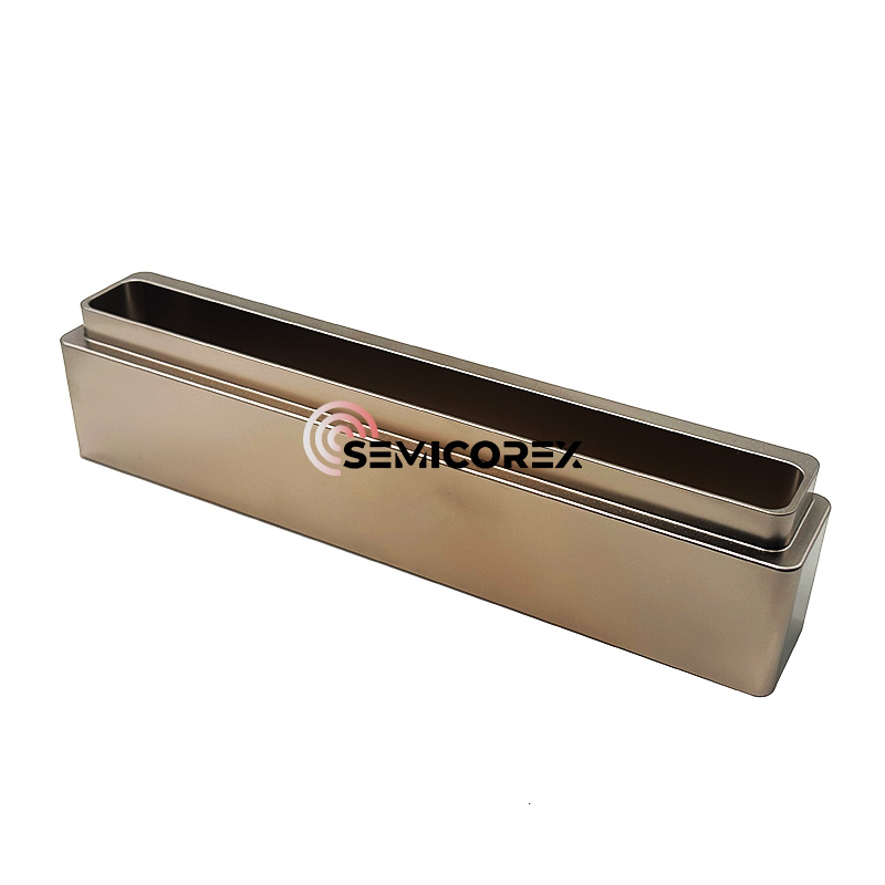
Semicorex Silicon Shield Ring is a high-purity silicon component engineered for advanced plasma etching systems, serving as both a protective shield and an auxiliary electrode. Semicorex ensures ultra-clean performance, process stability, and superior etching results with precision-engineered semiconductor components.*
Send Inquiry
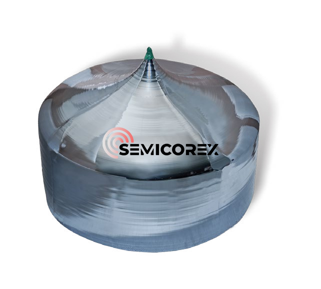
Semicorex Silicon Shield Ring is a critical semiconductor component in the etching process. Its primary function is to surround the electrode and prevent excessive plasma leakage. With a material purity exceeding 9N (99.9999999%), the shield ring can be made by both single-crystal and multi-crystal silicon, ensuring ultra-clean operation and reliable compatibility with advanced semiconductor manufacturing processes.
Accurate plasma control in the CCP/ICP etching process is essential for effective, uniform etch rate, and wafer quality. Uncontrolled plasma leakage outside of the desired etching area could create surface erosion and contamination or damage the components inside the chamber. The silicon shield ring is an effective, simple solution to this problem, created to form a protective barrier on the outside perimeter of the electrode, containment the plasma from spreading outside of the target area and restricting the etching to the desired area only. The silicon shield ring also acts as an outer electrode to stabilize the plasma distribution and enable more uniform energy at the wafer surface.

The thermal and electrical properties of silicon further support the performance of the Etching Shield Ring. Its resistance to high process temperatures provides structural integrity during prolonged plasma exposure, and its electrical conductivity allows the component to operate properly as an element in the electrode system. Together, these applications enhance plasma confinement and improve energy uniformity, which allow for repeatable etch profiles across wafers.
Mechanical tolerance is another notable characteristic of the Silicon Etching Shield Ring. By being manufactured to tight tolerances, it assures accurate positioning around the electrode and maintains spacing and geometry of the chamber. This mechanical precision generates repeatable process conditions for less variability between individual runs, and helps allow for high-volume semiconductor production. The material itself has excellent compatibility with plasma environments; therefore eroding its structure allows it to typically provide long service life and stability in process performance.
Durability and cost effectiveness are two more valuable benefits. By shielding unnecessary sections of the chamber from the plasma, the shield ring reduces wear on other critical components, which lessens maintenance efforts and increases overall operational uptime. Long service life and less frequent replacement make it a cost effective solution for semiconductor fabs to increase productivity and thereby reduce operating costs.
The Silicon shield ring can also be customized for each tool configuration and process specifications since they are available in several sizes and geometries to accommodate the many different plasma etching chambers that manufactures make, while still achieving optimal fit. Additionally, surface treatments and polishing can be utilized to further reduce particle generation for ultra-clean manufacturing standards.


