- English
- Español
- Português
- русский
- Français
- 日本語
- Deutsch
- tiếng Việt
- Italiano
- Nederlands
- ภาษาไทย
- Polski
- 한국어
- Svenska
- magyar
- Malay
- বাংলা ভাষার
- Dansk
- Suomi
- हिन्दी
- Pilipino
- Türkçe
- Gaeilge
- العربية
- Indonesia
- Norsk
- تمل
- český
- ελληνικά
- український
- Javanese
- فارسی
- தமிழ்
- తెలుగు
- नेपाली
- Burmese
- български
- ລາວ
- Latine
- Қазақша
- Euskal
- Azərbaycan
- Slovenský jazyk
- Македонски
- Lietuvos
- Eesti Keel
- Română
- Slovenski
- मराठी
- Srpski језик
News
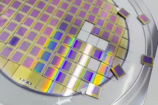
What is plasma dicing?
Wafer dicing is the final step in the semiconductor manufacturing process, separating silicon wafers into individual chips (also called dies). Plasma dicing uses a dry etching process to etch away the material in the dicing streets through fluorine plasma to achieve the separation effect. With the a......
Read MoreHow Ceramic Substrates Support Automotive Power Modules
The new energy vehicle industry is quickly advancing toward high-quality growth, becoming an eagerly awaited part of the global supply chain. The automotive power module acts as the "power center" of new energy vehicles, responsible for converting the battery's DC power into the AC needed to operate......
Read MoreWhat is the Chemical Vapor Deposition?
Chemical vapor deposition (CVD) is a coating technology that uses gaseous or vaporous substances to undergo chemical reactions in the gas phase or at a gas-solid interface to generate solid substances that are deposited on the substrate surface, thereby forming high-performance solid films. The core......
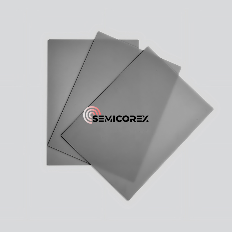
Read MoreWhat are the characteristics of black alumina ceramics
Black alumina, thanks to its unique light-blocking property, durability, electrical insulation, low density, high air tightness and chemical stability, has become a key material in high-end fields such as semiconductors, optics and aerospace, especially irreplaceable in scenarios that are sensitive ......
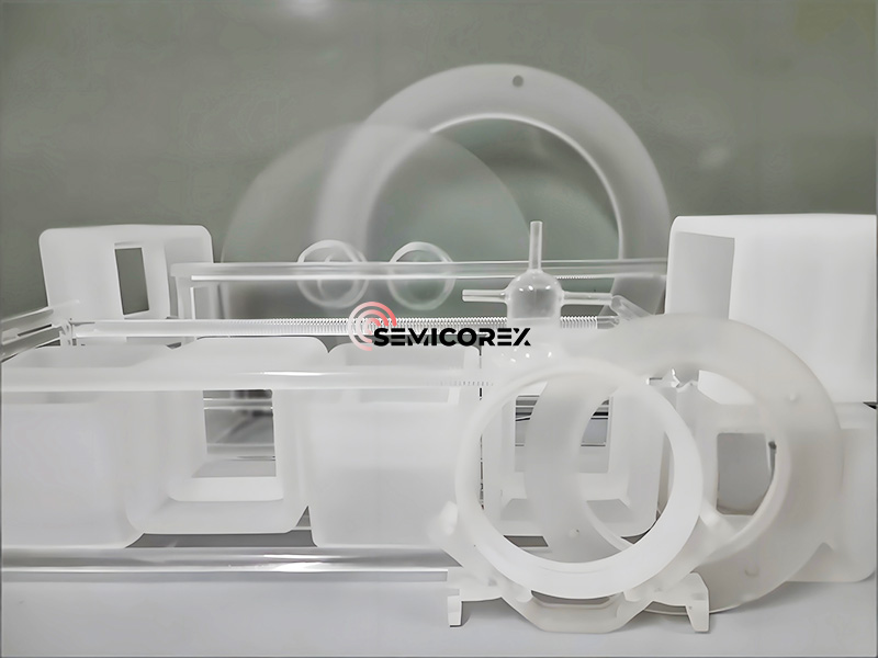
Read MoreWhat is the stress of quartz glass parts
Stress in quartz glass components refers to the uneven internal stress generated by various factors. Essentially, it's the stored elastic strain generated by the unbalanced forces acting on atoms or molecules within the material. This can cause microscopic distortions in the material structure, whic......
Read More


