
- English
- Español
- Português
- русский
- Français
- 日本語
- Deutsch
- tiếng Việt
- Italiano
- Nederlands
- ภาษาไทย
- Polski
- 한국어
- Svenska
- magyar
- Malay
- বাংলা ভাষার
- Dansk
- Suomi
- हिन्दी
- Pilipino
- Türkçe
- Gaeilge
- العربية
- Indonesia
- Norsk
- تمل
- český
- ελληνικά
- український
- Javanese
- فارسی
- தமிழ்
- తెలుగు
- नेपाली
- Burmese
- български
- ລາວ
- Latine
- Қазақша
- Euskal
- Azərbaycan
- Slovenský jazyk
- Македонски
- Lietuvos
- Eesti Keel
- Română
- Slovenski
- मराठी
- Srpski језик

What is plasma dicing?
What is plasma dicing?
Wafer dicing is the final step in the semiconductor manufacturing process, separating silicon wafers into individual chips (also called dies). Traditional methods use diamond blades or lasers to cut along the dicing streets between the chips, separating them from the wafer. Plasma dicing uses a dry etching process to etch away the material in the dicing streets through fluorine plasma to achieve the separation effect. With the advancement of semiconductor technology, the market is increasingly demanding smaller, thinner, and more complex chips. Plasma dicing is gradually replacing traditional diamond blades and laser solutions because it can improve yield, production capacity, and design flexibility, becoming the first choice of the semiconductor industry.
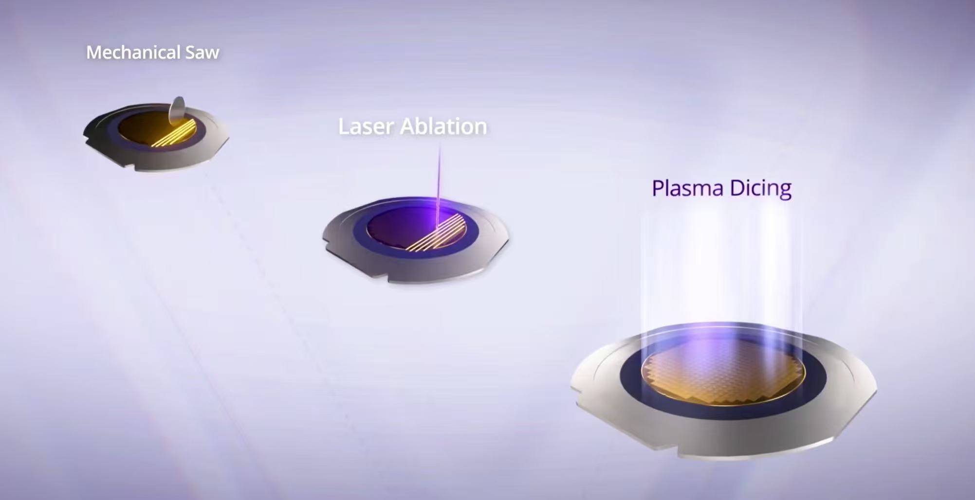
Plasma dicing uses chemical methods to remove materials in the dicing streets. There is no mechanical damage, no thermal stress, and no physical impact, so it will not cause damage to the chips. Therefore, chips separated using plasma have significantly higher fracture resistance than those dice using diamond blades or lasers. This improvement in mechanical integrity is particularly valuable for chips that are subject to physical stress during use.
Plasma dicing can greatly improve chip production efficiency and chip output per single wafer. Diamond blades and laser dicing require dicing along the scribe lines one by one, while plasma dicing can process all scribe lines simultaneously, which greatly improves the production efficiency of chips. Plasma dicing is not physically limited by the width of a diamond blade or the size of a laser spot, and can make the dicing streets narrower, allowing more chips to be cut from a single wafer. This cutting method frees wafer layout from the constraints of a straight-line cutting path, allowing for greater flexibility in chip shape and size design. This fully utilizes the wafer area, avoiding the situation in which the wafer area had to be sacrificed for mechanical dicing. This significantly increases chip output, especially for small-sized chips.
Mechanical dicing or laser ablation can leave debris and particulate contamination on the wafer surface, which is difficult to completely remove even with careful cleaning. The chemical nature of plasma dicing determines that it only produces gaseous byproducts that can be removed by a vacuum pump, ensuring that the wafer surface remains clean. This clean, non-mechanical contact separation is particularly suitable for fragile devices such as MEMS. There are no mechanical forces to vibrate the wafer and damage the sensing elements, and no particles to get stuck between components and affect their movement.
Despite its numerous advantages, plasma dicing also presents challenges. Its complex process requires high-precision equipment and experienced operators to ensure accurate and stable dicing. Moreover, the high temperature and energy of the plasma beam place higher demands on environmental control and safety precautions, increasing the difficulty and cost of its application.
Semicorex offers high-quality silicon wafers. If you need more details, please feel free to contact us at any time.


