
- English
- Español
- Português
- русский
- Français
- 日本語
- Deutsch
- tiếng Việt
- Italiano
- Nederlands
- ภาษาไทย
- Polski
- 한국어
- Svenska
- magyar
- Malay
- বাংলা ভাষার
- Dansk
- Suomi
- हिन्दी
- Pilipino
- Türkçe
- Gaeilge
- العربية
- Indonesia
- Norsk
- تمل
- český
- ελληνικά
- український
- Javanese
- فارسی
- தமிழ்
- తెలుగు
- नेपाली
- Burmese
- български
- ລາວ
- Latine
- Қазақша
- Euskal
- Azərbaycan
- Slovenský jazyk
- Македонски
- Lietuvos
- Eesti Keel
- Română
- Slovenski
- मराठी
- Srpski језик
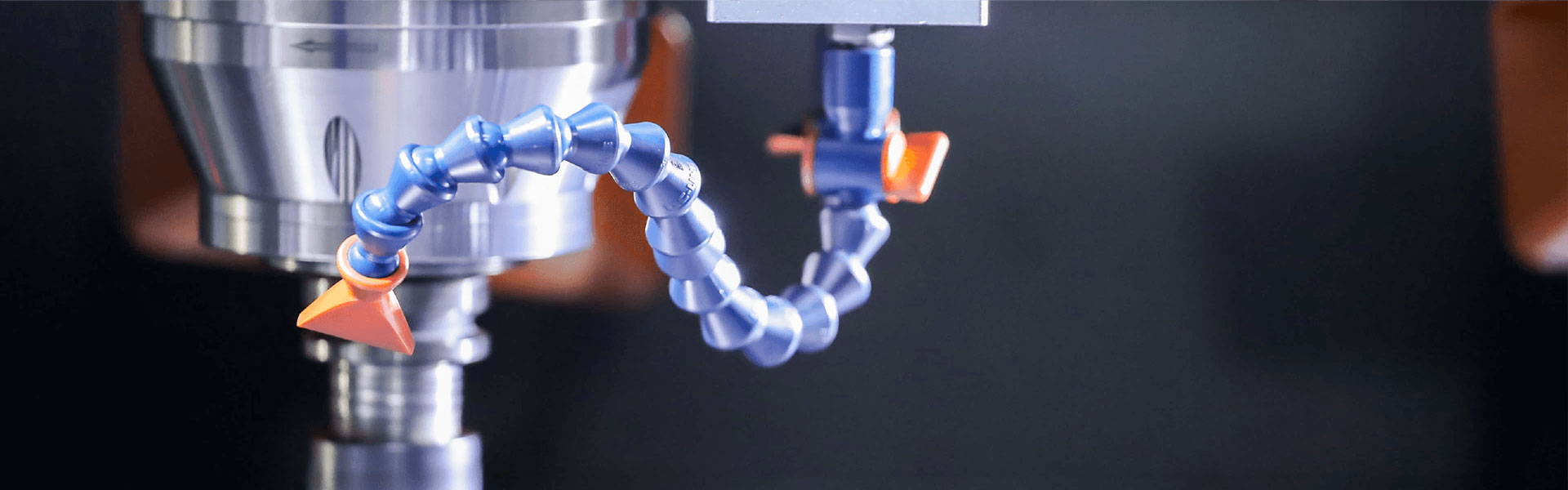
Semicorex SiC Components in High-temperature furnace
SiC ceramic is the high-temperature resistant material, which is durable in the semiconductor process. In the meanwhile, the material can be high purity to meet the semiconductor level.
Semicorex provides various customized SiC ceramic products, with 3D printing technology.
1. 3D printing allows for one-time molding of the entire shape, then sintering, all within a cleanroom, preventing the introduction of ionic contamination during the manufacturing process.
2. Traditional slip casting requires molds, and the demolding process can easily introduce contamination.
3. For the horizontal furnace tube with tail gas pipe, traditional slip casting requires separate molding and sintering of the furnace body and gas pipe, followed by a second sintering process before the gas nozzle can be bonded. This results in lower strength at the joint, making it prone to breakage.
4. Because 3D printing creates the entire shape before sintering, subsequent finishing significantly improves yield, especially for products requiring slots, such as wafer boats.
5. 3D printing also offers better density uniformity than conventional slip casting.
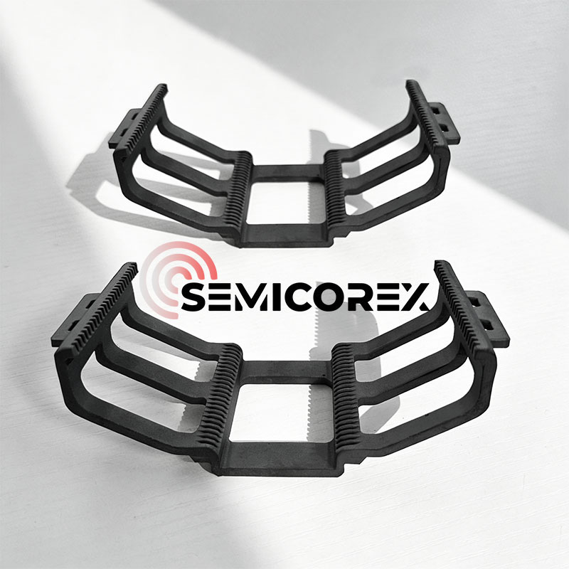
SiC Boats
A wafer boat is a process carrier used to hold wafers, primarily in high-temperature processing equipment.
In semiconductor manufacturing processes, wafers undergo multiple thermal processing steps, such as diffusion, oxidation, annealing, and chemical vapor deposition (CVD). During these processes, wafers are typically batched into furnace tube equipment, and the wafer boat serves the following functions:
- Carrying multiple wafers and maintaining a stable spacing;
- Ensuring the positional stability of wafers in high-temperature environments;
- Ensuring uniform gas flow in conjunction with the equipment.
The structure and material properties of the wafer boat directly affect the thermal field distribution and process consistency.
Silicon carbide wafer boats typically employ a frame design, offering high structural stability. Typical features include:
Multi-layer slot structure for precise wafer positioning;
Open design for easy gas flow between wafers;
High-rigidity frame to reduce the risk of deformation in high-temperature environments.
Depending on the equipment type, wafer boats can be designed as vertical or horizontal structures and support different wafer sizes (e.g., 6-inch, 8-inch, 12-inch).
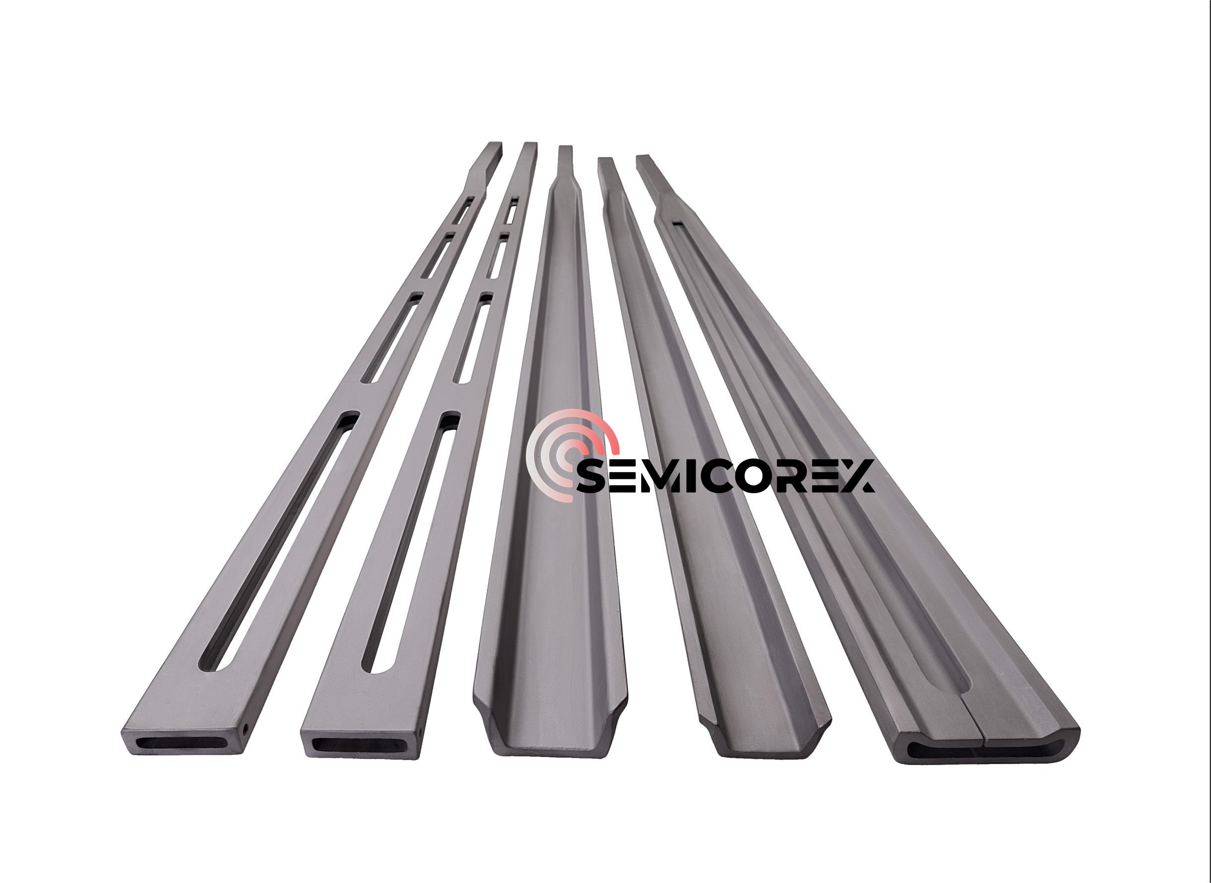
SiC Cantilever Paddles
In the photovoltaic energy manufacturing process, silicon wafers are placed on small boats, which are then placed on boat supports for thermal processes such as diffusion and LPCVD. The silicon carbide cantilever paddle is a key loading component that moves the boat support carrying the silicon wafers into and out of the heating furnace. The silicon carbide cantilever paddle ensures the concentricity of the silicon wafers and the furnace tubes, resulting in more uniform diffusion and passivation. It also remains pollution-free and deformation-free at high temperatures, exhibits excellent thermal shock resistance, and has a large load capacity, making it widely used in the photovoltaic cell field.
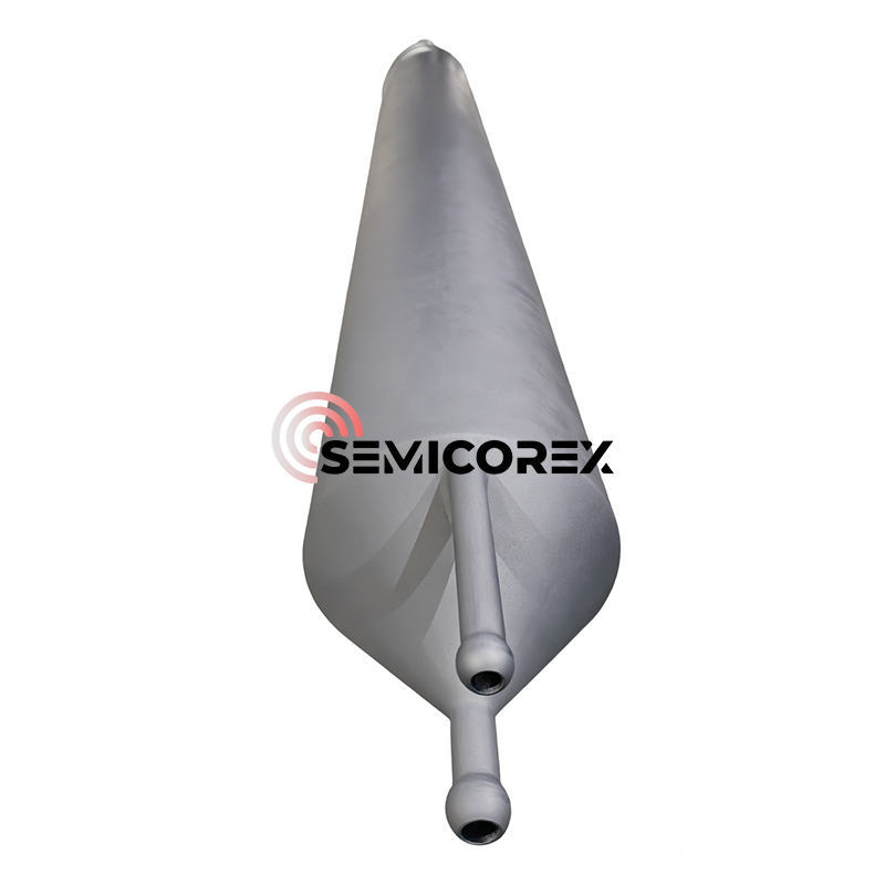
SiC Tubes
Furnace tubes are a key application in semiconductor manufacturing processes including thermal oxidation, diffusion doping, annealing, and chemical vapor deposition (LPCVD, APCVD). These processes are typically performed in high-temperature furnaces and encompass major steps in semiconductor manufacturing such as oxidation, impurity diffusion, and annealing for crystal defect repair.
Temperature oxidation is the most basic furnace tube process, involving heating a silicon wafer in an oxygen- or water-vapor environment. In microfabrication, thermal oxidation is a method of creating a thin layer of oxide (typically silicon dioxide) on the wafer surface. This technique forces an oxidant to diffuse into the wafer at high temperatures and react with it.
Diffusion doping is a core doping technique in semiconductor manufacturing. By driving impurity atoms (such as boron and phosphorus) to migrate into the semiconductor substrate (mainly silicon wafers) at high temperatures, it alters the local conductivity and resistivity of the substrate, thereby constructing key device structures such as PN junctions, base regions, and emitter regions.
Annealing processes primarily include rapid thermal annealing (RTA), a type of equipment that achieves high-temperature (300℃-1200℃) heat treatment within an extremely short time (seconds). It is widely used in key processes such as semiconductor dopant activation, silicide formation, and strain engineering. Its core technology lies in using halogen infrared lamps or laser sources to achieve rapid heating and cooling, eliminating internal wafer defects and optimizing the crystal structure, thereby improving semiconductor device performance.
Rapid thermal annealing furnaces offer a wide range of applications, such as annealing (RTA) of silicon and compound semiconductor wafers, rapid thermal oxidation (RTO), rapid thermal nitriding (RTN), rapid thermal diffusion of spin-coated dopants, crystallization, and contact alloying.
Previous:Carbon-based Thermal Field System