- English
- Español
- Português
- русский
- Français
- 日本語
- Deutsch
- tiếng Việt
- Italiano
- Nederlands
- ภาษาไทย
- Polski
- 한국어
- Svenska
- magyar
- Malay
- বাংলা ভাষার
- Dansk
- Suomi
- हिन्दी
- Pilipino
- Türkçe
- Gaeilge
- العربية
- Indonesia
- Norsk
- تمل
- český
- ελληνικά
- український
- Javanese
- فارسی
- தமிழ்
- తెలుగు
- नेपाली
- Burmese
- български
- ລາວ
- Latine
- Қазақша
- Euskal
- Azərbaycan
- Slovenský jazyk
- Македонски
- Lietuvos
- Eesti Keel
- Română
- Slovenski
- मराठी
- Srpski језик
Three Mainstream Focus Rings Comparison
Focus rings are precision annular parts typically installed around the wafer chuck of plasma etching equipment and are directly exposed to high-energy plasma during the etching process. Their core function is to act as sacrificial parts to secure uniform etching results across the entire wafer surface. Due to the edge effect, electric fields distort and diverge sharply at the wafer edges, making plasma density and energy vastly inconsistent with the wafer center, thus ruining etching uniformity. Focus rings resolve this issue via three core mechanisms as listed below:
1. Electric Field Optimization
Focus rings, placed around the wafer, act as an electric field buffer ramp to elevate the wafer’s physical and electrical boundaries. This setting evens out the plasma sheath at the wafer edge, directing ions to bombard the wafer surface at optimal angles, thereby ensuring consistent etching precision between the wafer edge and center.
2. Core Component Protection Mechanism
As sacrificial parts in etching system, focus rings bears the direct bombardment of high-energy plasma. They can shield expensive components underneath such as electrostatic chucks from damage, which greatly prolongs component longevity and reduces their maintenance expenses.
3. Thermal and Electrical Matching Maintenance
Some focus rings can facilitate achieving uniform heat distribution or forming a well-matched electric field with the wafer with tailored electrical conductivity, thus creating an extremely steady processing environment for high-precision etching.
Comparison of Three Widely Used Focus Ring Materials
Quartz, silicon and silicon carbide are the three dominant materials for manufacturing focus rings. Below is a detailed breakdown of their respective strengths, drawbacks and typical applications.
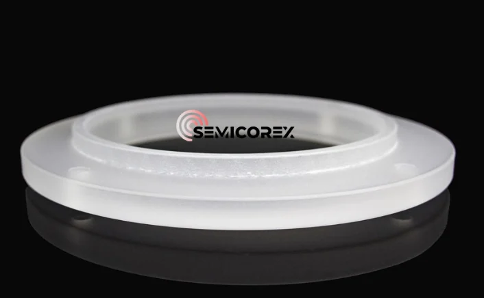
1. Quartz Focus Ring (Traditional Option)
A. Advantages and Drawbacks
Quartz focus rings exhibit low running cost, steady behavior in high-frequency fields and superior dielectric insulation in . Nevertheless, their limitations cannot be ignored. Quartz boasts low mechanical hardness, so quartz focus rings are prone to deformation under high-temperature conditions. They also deliver poor resistance to ion sputtering with an extremely high corrosion rate when exposed to fluorine-based plasma, which may cause contamination risks to production processes.
B. Suitable Scenarios
These rings work for non-high-bombardment RIE etchers supporting mid-to-low-end processes at 28nm and above. They cannot meet strict low-contamination and long-lifetime requirements for advanced nodes.
2. Silicon Focus Ring
A. Advantages and Drawbacks
Silicon focus rings are made of the same material as silicon wafers, offering well-matched thermal expansion coefficients and electrical properties. They tolerate temperatures up to 1600°C and help maintain even plasma distribution. Still, silicon performs poorly against fluorine plasma etching. It readily generates volatile SiF₄, wears down quickly and triggers frequent process drift and unplanned downtime. Frequent replacement is required—monocrystalline silicon rings usually need swapping every 10 to 12 days.
B. Suitable Scenarios
Silicon rings were once standard across semiconductor etching lines yet are gradually being replaced by SiC variants. They remain in use for cost-sensitive legacy mid-to-low-end manufacturing processes.
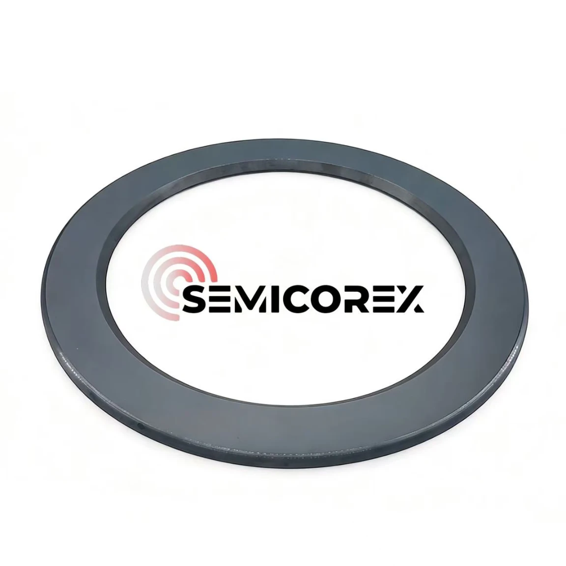
3. Silicon Carbide Focus Ring (Premium High-Performance Choice)
A. Advantages and Drawbacks
Silicon carbide focus rings boast a Mohs hardness of 9.5 and maintain a flexural strength of 500 to 600 MPa even at 1400°C. Meanwhile, their thermal expansion coefficient matches silicon wafers well, offering outstanding thermal shock resistance to withstand rapid thermal cycling, significantly optimizing etch uniformity at wafer edges. Most importantly, SiC boasts exceptional corrosion resistance against Ar, F, Cl and other plasma chemistries. Its etch rate in fluorine plasma is nearly zero. Silicon carbide focus rings deliver a service life 2–3 times longer than silicon versions, which greatly boosts overall equipment efficiency. CVD-grown high-purity silicon carbide reaches purity levels above 99.9995%, drastically cutting risks of particle and elemental contamination.
However, silicon carbide focus rings are not without drawbacks. Given silicon carbide’s extreme hardness, manufacturing silicon carbide focus rings requires diamond cutting tools. And their complex, lengthy machining procedures push up its initial purchase cost significantly.
B. Suitable Scenarios
Silicon carbide focus rings serve as the optimal option for advanced manufacturing processes including, sub-14nm logic chips and 3D NAND devices, and stand as the top material pick for silicon carbide power device fabrication.