
- English
- Español
- Português
- русский
- Français
- 日本語
- Deutsch
- tiếng Việt
- Italiano
- Nederlands
- ภาษาไทย
- Polski
- 한국어
- Svenska
- magyar
- Malay
- বাংলা ভাষার
- Dansk
- Suomi
- हिन्दी
- Pilipino
- Türkçe
- Gaeilge
- العربية
- Indonesia
- Norsk
- تمل
- český
- ελληνικά
- український
- Javanese
- فارسی
- தமிழ்
- తెలుగు
- नेपाली
- Burmese
- български
- ລາວ
- Latine
- Қазақша
- Euskal
- Azərbaycan
- Slovenský jazyk
- Македонски
- Lietuvos
- Eesti Keel
- Română
- Slovenski
- मराठी
- Srpski језик


Monocrystalline Silicon Planar Target
Monocrystalline silicon planar target from Semicorex is a crucial component in cutting-edge semiconductor manufacturing industry. Manufactured by top-quality monocrystalline silicon material, it features a highly ordered crystal structure and remarkable purity. These properties make it an ideal solution for manufacturing reliable, high-performance semiconductor films and optical films.
Send Inquiry
Product Description
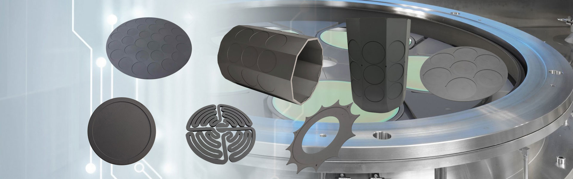
Monocrystalline silicon planar target is usually processed by high-precision cutting equipment from monocrystalline silicon ingots fabricated by the Czochralski method. To meet the diversification of customer needs, monocrystalline silicon planar target can be cut into desired shapes for your esteemed customers. The precise grinding and polishing processing technology ensures the superb surface flatness of the target material, providing a strong guarantee for the deposition of thin films.
Monocrystalline silicon planar target is placed inside in a vacuum reaction chamber together with the substrate to be coated during the film deposition process. When the monocrystalline silicon planar target is bombarded by high-energy ions, silicon atoms on its surface are sputtered off. These sputtered silicon atoms then migrate and deposit onto the surface of the substrate, eventually forming a silicon thin film.
Monocrystalline silicon planar target serves as the material source for thin-film deposition. All silicon atoms deposited onto the wafer surface originate from monocrystalline silicon planar targets. Therefore, the quality of the monocrystalline silicon planar target directly determines the purity, uniformity and other key properties of the deposited thin film.
The superb purity characteristic endows monocrystalline silicon planar target with the ability to prevent impurities from contaminating the thin film. This significantly improves the electrical performance of semiconductor devices. The improvement of the thin films’ uniformity and adhesion benefits from its highly ordered crystal structure, which enables the sputtering particles to migrate and deposit on the wafer surface more regularly. The planar structure design is suitable for large-area and high-speed sputtering requirements, and is applicable to large-scale production scenarios such as semiconductor wafers and display panels.
Hot Tags: Monocrystalline Silicon Planar Target, China, Manufacturers, Suppliers, Factory, Customized, Bulk, Advanced, Durable
Product Tag
Related Category
Wafer Heater
Chamber Lids
End Effector
Inlet Rings
Focus Ring
Wafer Chuck
Cantilever Paddle
Shower Head
Process Tube
Half Parts
Wafer Grinding Disk
Silicon Parts
Send Inquiry
Please feel free to give your inquiry in the form below. We will reply you in 24 hours.


