
- English
- Español
- Português
- русский
- Français
- 日本語
- Deutsch
- tiếng Việt
- Italiano
- Nederlands
- ภาษาไทย
- Polski
- 한국어
- Svenska
- magyar
- Malay
- বাংলা ভাষার
- Dansk
- Suomi
- हिन्दी
- Pilipino
- Türkçe
- Gaeilge
- العربية
- Indonesia
- Norsk
- تمل
- český
- ελληνικά
- український
- Javanese
- فارسی
- தமிழ்
- తెలుగు
- नेपाली
- Burmese
- български
- ລາວ
- Latine
- Қазақша
- Euskal
- Azərbaycan
- Slovenský jazyk
- Македонски
- Lietuvos
- Eesti Keel
- Română
- Slovenski
- मराठी
- Srpski језик
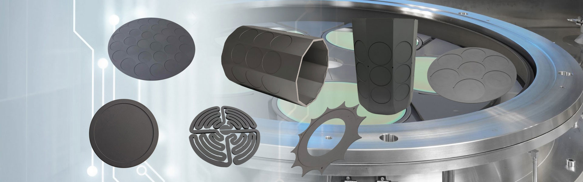


Customized Porous Ceramic chuck
Customized porous ceramic chuck is the superior workpiece clamping and fixing solution designed exclusively for semiconductor manufacturing. Selecting Semicorex means you will benefit from reliable quality, customization services and increased productivity.
Send Inquiry
Product Description
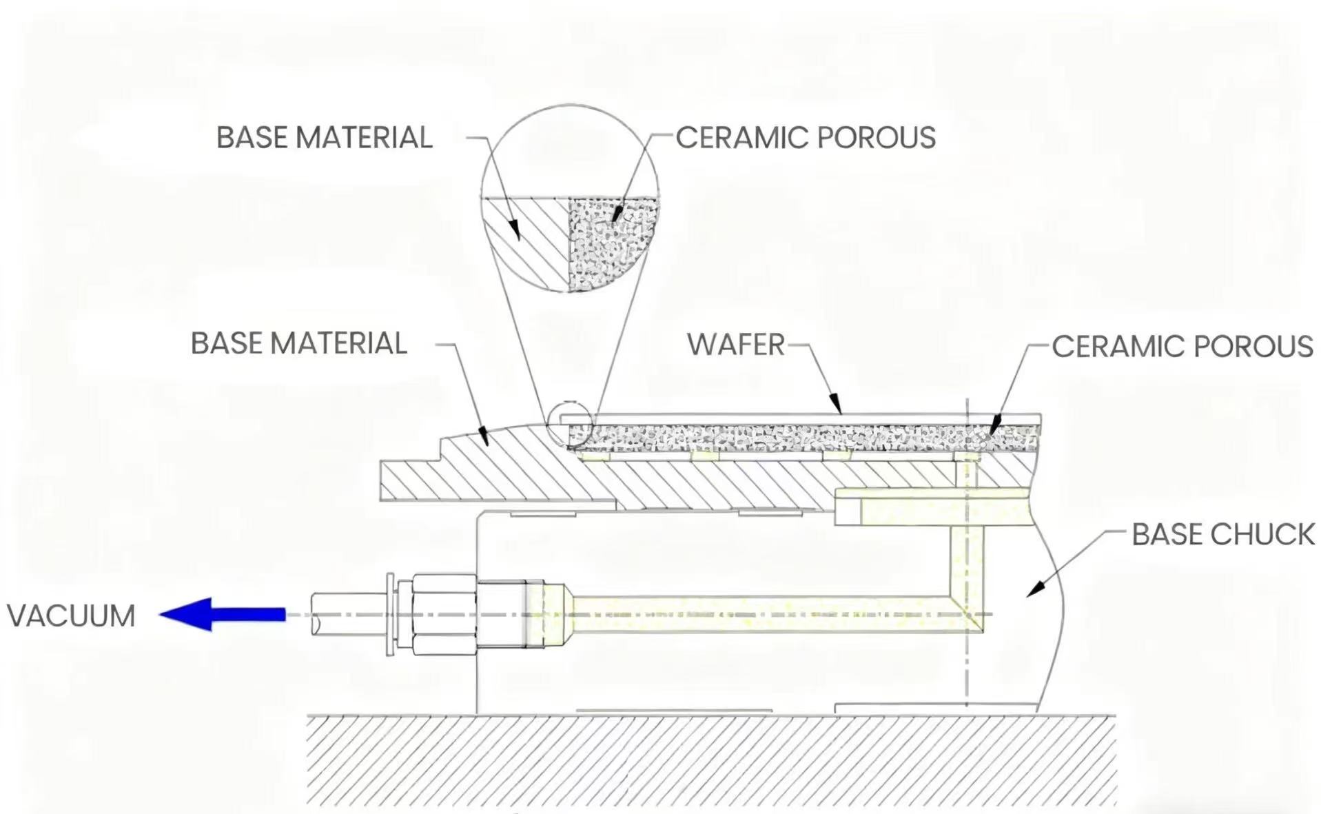
Customized porous ceramic chuck comprises the base and the porous ceramic plate. Connecting to a vacuum system, the low-pressure environment is created by evacuating the air between the wafer and the ceramic. Under vacuum negative pressure, the wafer is firmly adhered to the chuck surface, ultimately achieving safe and stable fixation and positioning.
Semicorex consistently prioritizes the fundamental needs of our valued customers while providing upscale and personalized services. We offer a diverse selection of options ensuring that the final customized porous ceramic chucks seamlessly adapt to workpieces of various shapes and sizes, thereby effectively enhancing equipment operating efficiency and production stability.
The specifications:
|
Size |
4-inch/6-inch/8-inch/12-inch |
|
Flatness |
2μm/2μm/3μm/3μm or above |
|
Material of porous ceramic plate |
Alumina and silicon carbide |
|
Pore size of porous ceramic |
5-50μm |
|
Porosity of porous ceramic |
35%-50% |
|
Anti-static function |
Optional |
|
Base material |
Stainless steel, aluminum alloy and ceramics(silicon carbide) |
Precision-machined customized porous ceramic chuck offers uniform adsorption force distribution across the workpiece surface, effectively preventng workpiece deformation or machining inaccuracies caused by uneven force application. Moreover, thanks to its strong chemical corrosion resistance and exceptional high-temperature resistance, the customized porous ceramic chuck maintains stable long-term operation in challenging and complex production environments.
The Application scenarios:
1. Semiconductor Manufacturing: Wafer processing such as wafer thinning, dicing, grinding, polishing; chemical vapor deposition (CVD) and physical vapor deposition (PVD) process; ion implantation.
2. Photovoltaic Cell Manufacturing: Silicon wafer dicing, coating, and packaging processes in photovoltaic cells.
3. Precision Machining: Clamping and fixing thin, fragile, or high-precision workpieces.
Hot Tags: Customized Porous Ceramic chuck, China, Manufacturers, Suppliers, Factory, Customized, Bulk, Advanced, Durable
Product Tag
Related Category
Wafer Heater
Chamber Lids
End Effector
Inlet Rings
Focus Ring
Wafer Chuck
Cantilever Paddle
Shower Head
Process Tube
Half Parts
Wafer Grinding Disk
Silicon Parts
Send Inquiry
Please feel free to give your inquiry in the form below. We will reply you in 24 hours.
Related Products


