
- English
- Español
- Português
- русский
- Français
- 日本語
- Deutsch
- tiếng Việt
- Italiano
- Nederlands
- ภาษาไทย
- Polski
- 한국어
- Svenska
- magyar
- Malay
- বাংলা ভাষার
- Dansk
- Suomi
- हिन्दी
- Pilipino
- Türkçe
- Gaeilge
- العربية
- Indonesia
- Norsk
- تمل
- český
- ελληνικά
- український
- Javanese
- فارسی
- தமிழ்
- తెలుగు
- नेपाली
- Burmese
- български
- ລາວ
- Latine
- Қазақша
- Euskal
- Azərbaycan
- Slovenský jazyk
- Македонски
- Lietuvos
- Eesti Keel
- Română
- Slovenski
- मराठी
- Srpski језик
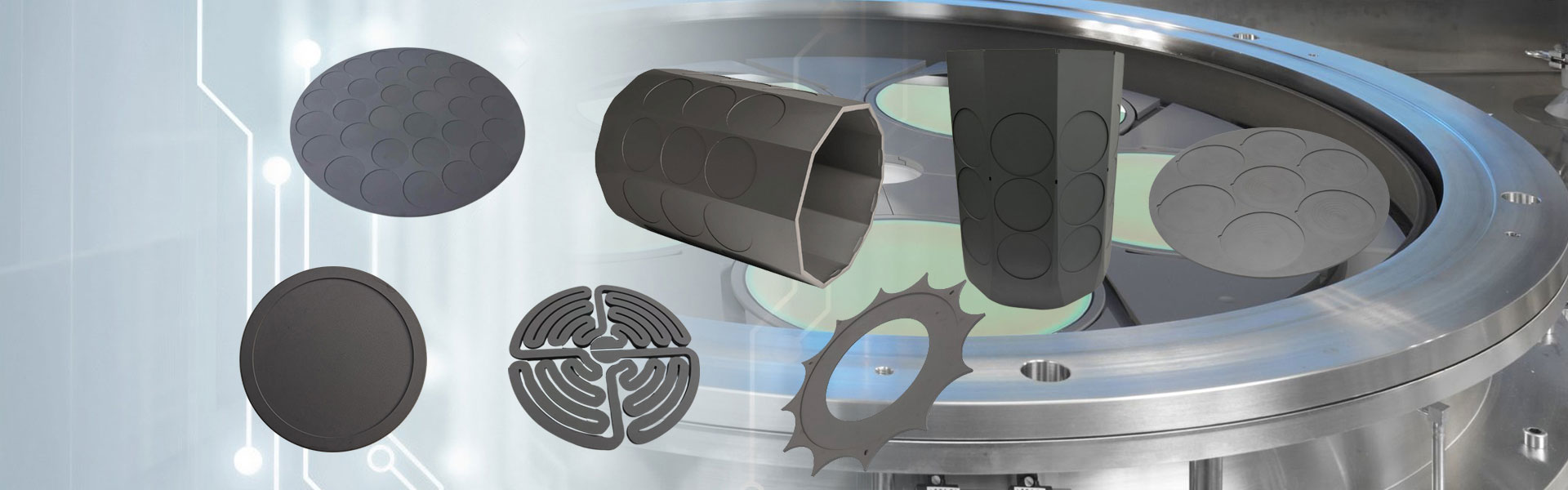


Ceramic Electrostatic Chucks
Semicorex ceramic electrostatic chucks are precision electrostatic adsorption components made of high-performance alumina and aluminum nitride ceramics, which uses the principle of electrostatic adsorption to clamp and fix wafers. It is widely used in semiconductor manufacturing fields. Semicorex has advanced technology, high-quality materials, and cost-effective products. We look forward to becoming your reliable supply partner in China.
Send Inquiry
Product Description
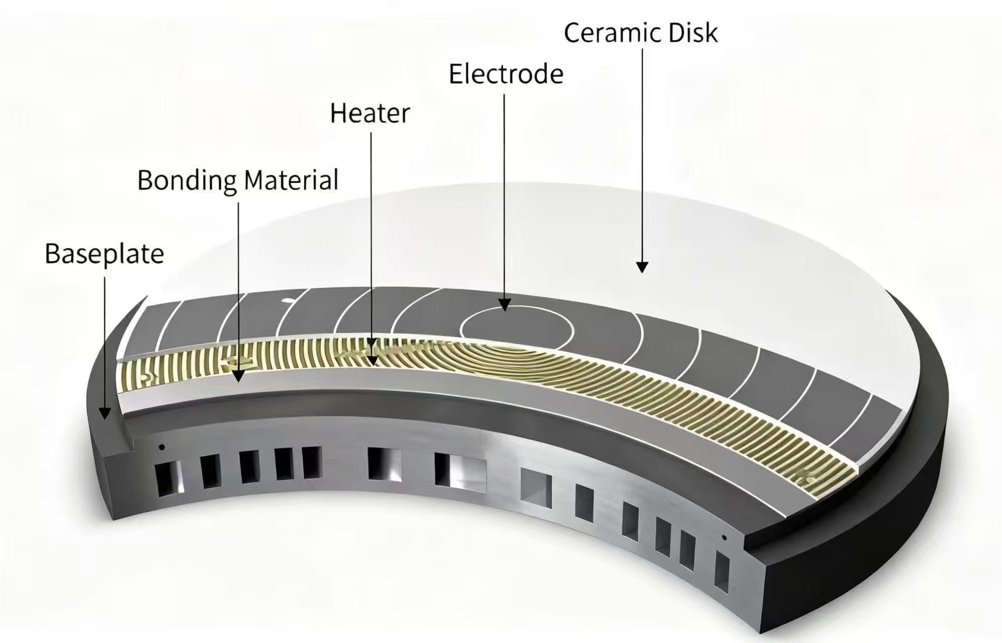
Ceramic electrostatic chucks are precision components that use the electrostatic field generated between electrodes and wafers to clamp and fix wafers. They are widely applied in fields such as semiconductors, flat panel displays, and optics, and are core components of high-end equipment like PVD devices, etching machines, and ion implanters.
Compared with traditional mechanical chucks and vacuum chucks, ceramic electrostatic chucks have many advantages in semiconductor manufacturing field. This ceramic electrostatic chuck uses static electricity to flatten and evenly hold wafers on its surface. This uniform adsorption force can keep the adsorbed object relatively flat, avoiding wafer warping or deformation that may be caused by traditional mechanical chucks or vacuum chucks, and ensuring that the wafer maintains processing accuracy suitable for high-precision semiconductor processes.
Some ceramic electrostatic chucks have integrated heating functions, which can accurately control the wafer temperature through back-blowing gas or internal heating electrodes, adapt to the strict temperature requirements of different processes, and improve processing stability.
Unlike mechanical chucks, ceramic electrostatic chucks reduce mechanical moving parts, reduce the impact of particulate contaminants on wafer quality, effectively protect the cleanliness of the wafer surface, and improve product yield.
Ceramic electrostatic chucks offer broad compatibility. They can accommodate wafers of varying sizes and materials, including silicon, gallium arsenide, and silicon carbide, meeting diverse semiconductor manufacturing needs.
They can work stably in high vacuum environments such as ion implantation and CVD, overcoming the limitation of traditional vacuum chucks that cannot absorb wafers in a vacuum environment, and perfectly meeting the process requirements of ion implantation, chemical vapor deposition (CVD) and other processes in semiconductor manufacturing.
Hot Tags: Ceramic Electrostatic Chucks, China, Manufacturers, Suppliers, Factory, Customized, Bulk, Advanced, Durable
Product Tag
Related Category
Silicon Carbide (SiC)
Alumina (Al2O3)
Silicon Nitride (Si3N4)
Aluminum Nitride (AIN)
Zirconia (ZrO2)
Composite Ceramic
Axle Sleeve
Bushing
Wafer Carrier
Mechanical Seal
Wafer Boat
Send Inquiry
Please feel free to give your inquiry in the form below. We will reply you in 24 hours.


