
- English
- Español
- Português
- русский
- Français
- 日本語
- Deutsch
- tiếng Việt
- Italiano
- Nederlands
- ภาษาไทย
- Polski
- 한국어
- Svenska
- magyar
- Malay
- বাংলা ভাষার
- Dansk
- Suomi
- हिन्दी
- Pilipino
- Türkçe
- Gaeilge
- العربية
- Indonesia
- Norsk
- تمل
- český
- ελληνικά
- український
- Javanese
- فارسی
- தமிழ்
- తెలుగు
- नेपाली
- Burmese
- български
- ລາວ
- Latine
- Қазақша
- Euskal
- Azərbaycan
- Slovenský jazyk
- Македонски
- Lietuvos
- Eesti Keel
- Română
- Slovenski
- मराठी
- Srpski језик
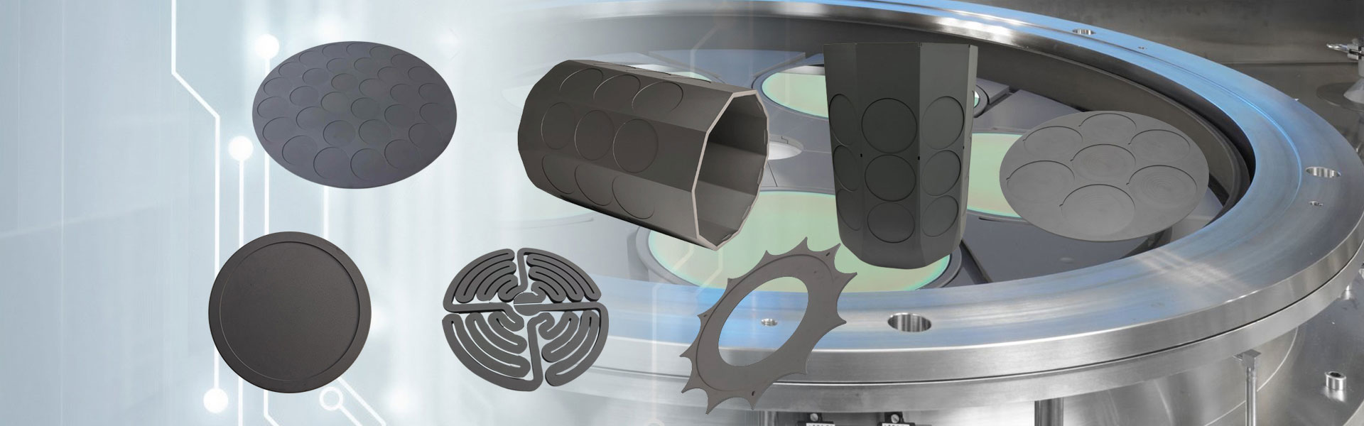


Glass Wafers
Semicorex glass wafers are circular thin slices made from semiconductor-grade glass. Due to their exceptional high-temperature resistance, strength corrosion resistance, excellent mechanical properties, and high light transmission efficiency, they are widely used in precision manufacturing fields such as semiconductors, optics, biotechnology, microelectronics, and integrated circuit (IC) packaging.
Send Inquiry
Product Description
The mainstream processing method of glass wafers includes vacuum electric fusion, gas melting and chemical vapor deposition. Semicorex commonly uses a specific processing method tailored to different application requirements of glass wafers. To perfectly meet the stringent requirements of the high-end precision manufacturing industry, Semicorex glass wafers employs advanced laser measurement equipment to rigorously control the size, thickness, and surface quality of each wafer after finishing processes such as grinding and polishing.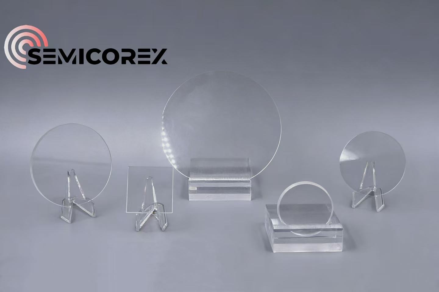
The Excellent Characteristics
1. Strength corrosion resistance
2. Superior thermal stability
3. Low surface roughness
4. High light transmission efficiency
5. Excellent mechanical properties
6. Remarkable electrical performance
The Applications of Semicorex Glass Wafers
1. Semiconductors industry:
Glass wafers serve as carriers or packaging substrates for silicon wafers, and are used in advanced packaging such as wafer-level packaging (WLP), fan-out wafer-level packaging (FOWLP), and chip stacking to improve the performance and integration of semiconductor chips.
2. Optical field:
Thanks to their high light transmission efficiency, low surface roughness, and excellent optical uniformity, glass wafers are commonly applied in the manufacture of optical components such as lenses, prisms, and waveguides, playing a crucial role in AR/VR glasses, laser devices, and optical sensors.
3. Biomedical field:
In addition to being used as essential components in medical optical instruments such as ophthalmic equipment, endoscopes, and laser therapy devices, glass wafers are also used in biomedical devices such as DNA sequencing chips, PCR reactors, and microfluidic chips, providing technical support for disease diagnosis, gene sequencing, and precision medicine.
4. Applications of microelectromechanical systems
Glass wafers are used as packaging materials or substrates for MEMS devices to provide the sealed environment to protect the internal microstructures, which are commonly used in pressure sensors, accelerometers, optical MEMS, and other fields.
Hot Tags: Glass Wafers, China, Manufacturers, Suppliers, Factory, Customized, Bulk, Advanced, Durable
Product Tag
Related Category
Send Inquiry
Please feel free to give your inquiry in the form below. We will reply you in 24 hours.


