
- English
- Español
- Português
- русский
- Français
- 日本語
- Deutsch
- tiếng Việt
- Italiano
- Nederlands
- ภาษาไทย
- Polski
- 한국어
- Svenska
- magyar
- Malay
- বাংলা ভাষার
- Dansk
- Suomi
- हिन्दी
- Pilipino
- Türkçe
- Gaeilge
- العربية
- Indonesia
- Norsk
- تمل
- český
- ελληνικά
- український
- Javanese
- فارسی
- தமிழ்
- తెలుగు
- नेपाली
- Burmese
- български
- ລາວ
- Latine
- Қазақша
- Euskal
- Azərbaycan
- Slovenský jazyk
- Македонски
- Lietuvos
- Eesti Keel
- Română
- Slovenski
- मराठी
- Srpski језик

What are rings in etching
In chip manufacturing, photolithography and etching are two closely linked steps. Photolithography precedes etching, where the circuit pattern is developed on the wafer using photoresist. Etching then removes the film layers not covered by the photoresist, completing the transfer of the pattern from the mask to the wafer and preparing for subsequent steps like ion implantation.
Etching involves the selective removal of unnecessary material using chemical or physical methods. Following coating, resist coating, photolithography, and development, etching removes unnecessary thin film material exposed on the wafer surface, leaving only the desired areas. Excess photoresist is then removed. Repeating these steps repeatedly creates complex integrated circuits. Because etching involves material removal, it is called a "subtractive process."
Dry etching, also known as plasma etching, is the dominant method in semiconductor etching. Plasma etchers are broadly classified into two categories based on their plasma generation and control technologies: capacitively coupled plasma (CCP) etching and inductively coupled plasma (ICP) etching. CCP etchers are primarily used for etching dielectric materials, while ICP etchers are primarily used for etching silicon and metals, and are also known as conductor etchers. Dielectric etchers target dielectric materials such as silicon oxide, silicon nitride, and hafnium dioxide, while conductor etchers target silicon materials (single crystal silicon, polycrystalline silicon, and silicide, etc.) and metal materials (aluminum, tungsten, etc.).
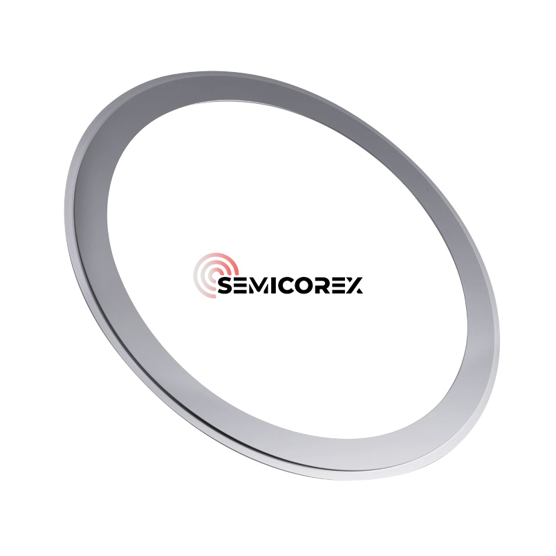
In the etching process, we will primarily use two types of rings: focus rings and shield rings.
Due to the edge effect of plasma, the density is higher at the center and lower at the edges. The focus ring, through its annular shape and the material properties of CVD SiC, generates a specific electric field. This field guides and confines the charged particles (ions and electrons) in the plasma to the wafer surface, particularly at the edge. This effectively raises the plasma density at the edge, bringing it closer to that at the center. This significantly improves etching uniformity across the wafer, reduces edge damage, and increases yield.
Typically located outside the electrode, its primary function is to block plasma overflow. Depending on the structure, it may also function as part of the electrode. Common materials include CVD SiC or single-crystal silicon.
Semicorex offers high-quality CVD SiC and Silicon Etching rings based on customers’ needs. If you have any inquiries or need additional details, please don't hesitate to get in touch with us.
Contact phone # +86-13567891907
Email: sales@semicorex.com
Previous:What is plasma dicing?


