
- English
- Español
- Português
- русский
- Français
- 日本語
- Deutsch
- tiếng Việt
- Italiano
- Nederlands
- ภาษาไทย
- Polski
- 한국어
- Svenska
- magyar
- Malay
- বাংলা ভাষার
- Dansk
- Suomi
- हिन्दी
- Pilipino
- Türkçe
- Gaeilge
- العربية
- Indonesia
- Norsk
- تمل
- český
- ελληνικά
- український
- Javanese
- فارسی
- தமிழ்
- తెలుగు
- नेपाली
- Burmese
- български
- ລາວ
- Latine
- Қазақша
- Euskal
- Azərbaycan
- Slovenský jazyk
- Македонски
- Lietuvos
- Eesti Keel
- Română
- Slovenski
- मराठी
- Srpski језик


LNOI Wafer
Semicorex LNOI Wafer: High-performance Lithium Niobate on Insulator wafers with customizable substrates for advanced photonics and RF applications. With precision engineering, customizable options, and superior material quality, Semicorex ensures high-performance LNOI wafers tailored to your application needs.*
Send Inquiry
Product Description
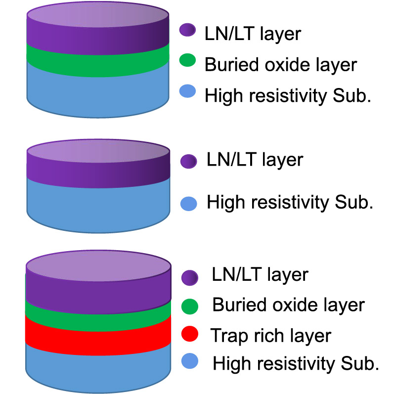
Semicorex offers premium Lithium Niobate on Insulator (LNOI wafer) with a thickness range of 0.3 to 50 μm, catering to advanced photonics, RF, and quantum applications. Our wafers come in 6-inch and 8-inch sizes, ensuring compatibility with modern semiconductor fabrication processes.Our LNOI wafer features precisely oriented X, Z, Y-42 cut lithium niobate films, enabling optimal electro-optic, piezoelectric, and nonlinear optical properties. The insulator and substrate layers can be customized to meet specific application needs, with options including Si, SiC, sapphire, spinel, and quartz.
Lithium niobate (LN) crystals possess exceptional electro-optical, acousto-optical, nonlinear optical, photorefractive, piezoelectric, ferroelectric, photoelastic, and pyroelectric properties. They are known for their stable mechanical characteristics and a wide transparent window (0.3-5 µm), making them widely utilized in integrated optics. Traditional methods for preparing optical waveguides from lithium niobate crystals, such as ion implantation, proton exchange, and titanium diffusion, result in a small refractive index difference and a large waveguide bending radius. This leads to larger device sizes, which limits their application in integrated optics.
Conversely, lithium niobate thin films (LNOI wafers) offer a significant refractive index contrast, enabling waveguides to have bending radii of only tens of microns and submicron cross-sections. This allows for high-density photon integration and strong light confinement, enhancing the interaction between light and matter.
LNOI wafers can be prepared using various techniques, including pulsed laser deposition, gel-gel methods, RF magnetron sputtering, and chemical vapor deposition. However, LNOI produced from these techniques often exhibits a polycrystalline structure, leading to increased light transmission loss. Additionally, there is a considerable gap between the physical properties of the film and those of single-crystal LN, which negatively impacts the performance of photonic devices.
The optimal method for preparing LNOI wafers involves a combination of processes such as ion implantation, direct bonding, and thermal annealing, which physically peel off the LN film from the bulk LN material and transfer it to a substrate. Grinding and polishing techniques can also yield high-quality LNOI. This approach minimizes damage to the LN crystal lattice during ion implantation and maintains crystal quality, provided that strict control is exercised over the uniformity of the film thickness. LNOI wafers not only retain essential properties like electro-optical, acousto-optic, and nonlinear optical characteristics but also maintain a single crystal structure, which is beneficial for achieving low optical transmission loss.
Optical waveguides are fundamental devices in integrated photonics, and various methods exist for their preparation. Waveguides on LNOI wafers can be established using traditional techniques such as proton exchange. Since LN is chemically inert, to avoid etching, easily etched materials can be deposited onto the LNOI to create loading strip waveguides. The materials suitable for loading strips include TiO2, SiO2, SiNx, Ta2O5, chalcogenide glass, and silicon. An LNOI optical waveguide created using the chemical mechanical polishing method has achieved a propagation loss of 0.027 dB/cm; however, its shallow waveguide sidewall complicates the realization of waveguides with small bending radii. The LNOI wafer waveguide, prepared using a plasma etching method, achieved a transmission loss of just 0.027 dB/cm. This represents a significant milestone, indicating that large-scale photon integration and single-photon-level processing can be realized. In addition to optical waveguides, numerous high-performance photonic devices have been developed on LNOI, including micro-ring/micro-disk resonators, end and grating couplers, and photonic crystals. A variety of functional photonic devices have also been successfully created. Leveraging the exceptional electro-optical and nonlinear optical effects of lithium niobate (LN) crystals allows for high-bandwidth optoelectronic modulation, efficient nonlinear conversion, and electro-optically controllable optical frequency comb generation, among other photonic functionalities. LN also exhibits an acousto-optic effect. The acousto-optic Mach-Zehnder modulator prepared on LNOI utilizes optomechanical interactions in the suspended lithium niobate film to convert a microwave signal with a frequency of 4.5 GHz into light at a wavelength of 1500 nm, facilitating efficient microwave-to-optical signal conversion.
Additionally, the acousto-optic modulator fabricated on LN film above a sapphire substrate avoids the need for a suspension structure due to the high sound velocity of sapphire, which also helps reduce acoustic wave energy leakage. The integrated acousto-optic frequency shifter developed on LNOI demonstrates higher frequency shift efficiency compared to those fabricated on aluminum nitride film. Advances have also been made in lasers and amplifiers using rare earth-doped LNOI. However, the rare earth-doped regions of LNOI wafers exhibit significant light absorption in the communication optical band, which hinders large-scale photonic integration. Exploring local rare earth doping on LNOI could provide a solution to this issue. Amorphous silicon can be deposited on LNOI to create photodetectors. The resulting metal-semiconductor and metal photodetectors show a responsivity of 22-37 mA/W across wavelengths of 635-850 nm. Simultaneously, heterogeneously integrating III-V semiconductor lasers and detectors on LNOI presents another viable solution for developing lasers and detectors on this material. However, the preparation process is complex and costly, necessitating improvements to reduce costs and increase the success rate.
Hot Tags: LNOI Wafer, China, Manufacturers, Suppliers, Factory, Customized, Bulk, Advanced, Durable
Product Tag
Related Category
Send Inquiry
Please feel free to give your inquiry in the form below. We will reply you in 24 hours.


