
- English
- Español
- Português
- русский
- Français
- 日本語
- Deutsch
- tiếng Việt
- Italiano
- Nederlands
- ภาษาไทย
- Polski
- 한국어
- Svenska
- magyar
- Malay
- বাংলা ভাষার
- Dansk
- Suomi
- हिन्दी
- Pilipino
- Türkçe
- Gaeilge
- العربية
- Indonesia
- Norsk
- تمل
- český
- ελληνικά
- український
- Javanese
- فارسی
- தமிழ்
- తెలుగు
- नेपाली
- Burmese
- български
- ລາວ
- Latine
- Қазақша
- Euskal
- Azərbaycan
- Slovenský jazyk
- Македонски
- Lietuvos
- Eesti Keel
- Română
- Slovenski
- मराठी
- Srpski језик
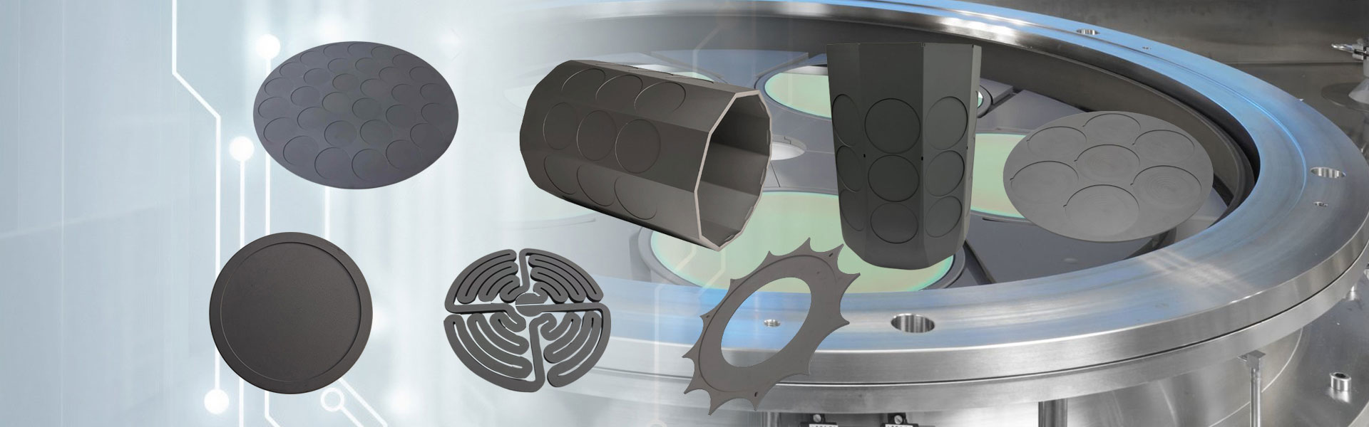


Upper Electrode Grounding Ring
Semicorex Upper Electrode Grounding Ring is an ultra-high-purity CVD SiC plasma control component that stabilizes electrical potential and supports uniform plasma distribution in advanced semiconductor etching and deposition systems. Semicorex supplies precision CVD SiC grounding rings and plasma-facing semiconductor components worldwide, offering customized dimensions, electrical properties, and reliable global delivery for leading semiconductor equipment manufacturers.*
Send Inquiry
Product Description
In modern semiconductor plasma processing equipment, maintaining electrical stability is just as important as controlling temperature, gas flow, and chamber pressure. Semicorex Upper Electrode Grounding Ring is a critical plasma-facing component designed to regulate electrical potential, stabilize plasma distribution, and support uniform wafer processing within etching and deposition chambers.
Manufactured from ultra-high-purity Chemical Vapor Deposition (CVD) Silicon Carbide (SiC), Semicorex Upper Electrode Grounding Ring operates in direct exposure to plasma and reactive process environments. Its exceptional purity, dimensional stability, and electrical performance make it an essential component for advanced integrated circuit fabrication, memory manufacturing, and power semiconductor production.
Semicorex provides precision-engineered CVD SiC Grounding Rings with superior material quality, extended service life, and customized electrical properties for next-generation semiconductor equipment.

The Role of the Upper Electrode Grounding Ring
Plasma reactors rely on carefully controlled electromagnetic fields to generate and sustain stable plasma conditions. During processing, the upper electrode assembly must maintain a balanced electrical environment to ensure consistent ion energy distribution across the wafer surface.
The Upper Electrode Grounding Ring functions as a precision grounding interface positioned around the upper electrode region. Its primary responsibilities include:
Stabilizing chamber electrical potential
Supporting uniform plasma generation
Reducing localized electric field distortion
Enhancing wafer processing consistency
Improving plasma confinement efficiency
Minimizing process variation between wafers
Without proper grounding control, plasma instability can negatively affect etching profiles, deposition uniformity, and overall production yield.
Ultra-High Purity CVD Silicon Carbide
The performance of plasma-facing components is highly dependent on material purity and structural integrity.
Semicorex Upper Electrode Grounding Rings are manufactured from ultra-high-purity CVD Silicon Carbide with purity levels reaching:
≥ 99.9995% SiC
This extremely high purity minimizes contamination risks within the chamber and supports advanced semiconductor manufacturing processes where even trace impurities can impact device performance.
Key advantages include:
Superior plasma erosion resistance
Reduced wear rates
Lower particle contamination
Extended maintenance intervals
Improved chamber uptime
Under typical operating conditions, the service life of a CVD SiC Grounding Ring can reach:
3 to 5 times longer than conventional silicon components
This extended lifespan reduces replacement frequency and lowers overall ownership costs for semiconductor manufacturers.
Electrical Performance Tailored to Process Requirements
Different plasma systems require different electrical characteristics to achieve optimal performance.
Semicorex offers customizable resistivity ranges to support various equipment architectures and chamber designs:
Electrical Resistivity Range:
0.5 – 10⁶ Ω·cm
This broad range allows engineers to select the most appropriate electrical properties for:
Plasma etching systems
Dielectric etch processes
Conductive film processing
Deposition chambers
Advanced RF plasma applications
Customized electrical behavior helps improve chamber stability and process repeatability.
Precision Manufacturing for Semiconductor Equipment
Upper Electrode Grounding Rings typically feature large diameters and tight dimensional tolerances.
A common production configuration includes:
Outer Diameter (OD): approximately 400 mm
Thickness range: 1–10 mm
Precision-machined geometry
Defect-free surface structure
Every component undergoes strict manufacturing control to ensure:
Uniform density
Accurate dimensions
Consistent electrical properties
Structural reliability
Semiconductor-grade cleanliness
The defect-free construction is essential for maintaining stable plasma operation and minimizing contamination risks.
Applications
Upper Electrode Grounding Rings are widely used in:
Plasma etching equipment
ICP etching systems
CCP plasma reactors
Semiconductor deposition chambers
Advanced logic manufacturing
DRAM and NAND production
Power semiconductor fabrication
Compound semiconductor processing
Their ability to combine electrical stability with exceptional plasma resistance makes them indispensable in modern semiconductor tools.
Why Choose Semicorex?
Semicorex combines advanced CVD SiC technology, precision machining expertise, and semiconductor-grade quality control to deliver grounding rings that meet the most demanding industry standards.
Our engineering team supports customized dimensions, resistivity specifications, surface treatments, and application-specific designs to ensure seamless integration with customer equipment platforms.
Hot Tags: Upper Electrode Grounding Ring, China, Manufacturers, Suppliers, Factory, Customized, Bulk, Advanced, Durable
Product Tag
Related Category
Silicon Carbide Coated
CVD SiC
Semiconductor Components
TaC Coating
Specialty Graphite
Ceramic
Quartz
Wafer
CVD Furnace
Other Semiconductor Material
UHTCMC
Send Inquiry
Please feel free to give your inquiry in the form below. We will reply you in 24 hours.


