
- English
- Español
- Português
- русский
- Français
- 日本語
- Deutsch
- tiếng Việt
- Italiano
- Nederlands
- ภาษาไทย
- Polski
- 한국어
- Svenska
- magyar
- Malay
- বাংলা ভাষার
- Dansk
- Suomi
- हिन्दी
- Pilipino
- Türkçe
- Gaeilge
- العربية
- Indonesia
- Norsk
- تمل
- český
- ελληνικά
- український
- Javanese
- فارسی
- தமிழ்
- తెలుగు
- नेपाली
- Burmese
- български
- ລາວ
- Latine
- Қазақша
- Euskal
- Azərbaycan
- Slovenský jazyk
- Македонски
- Lietuvos
- Eesti Keel
- Română
- Slovenski
- मराठी
- Srpski језик

Why Is a Customized Porous Ceramic Chuck the Ultimate Solution for High-Precision Semiconductor Manufacturing
As semiconductor devices become smaller, thinner, and more complex, wafer handling technologies must achieve unprecedented levels of precision and stability. A Customized Porous Ceramic Chuck has emerged as a critical component in advanced semiconductor manufacturing, offering uniform vacuum adsorption, excellent thermal stability, and superior flatness control.
Developed with industry-specific requirements in mind, Semicorex Customized Porous Ceramic Chuck solutions provide tailored designs for wafer processing, inspection, lithography, etching, and deposition applications. This article explores the structure, working principles, advantages, customization possibilities, application scenarios, and selection criteria of porous ceramic chucks while highlighting why they have become indispensable in modern semiconductor production.
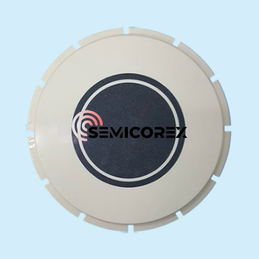
Table of Contents
- What Is a Customized Porous Ceramic Chuck?
- How Does a Porous Ceramic Chuck Work?
- Key Advantages of Customized Porous Ceramic Chucks
- Customization Options Available
- Major Applications in Semiconductor Manufacturing
- Porous Ceramic Chuck vs Traditional Vacuum Chuck
- How to Choose the Right Customized Porous Ceramic Chuck
- Future Trends in Porous Ceramic Chuck Technology
- Frequently Asked Questions
- Conclusion
What Is a Customized Porous Ceramic Chuck?
A Customized Porous Ceramic Chuck is a high-performance wafer holding device designed to secure semiconductor wafers through vacuum adsorption distributed uniformly across a porous ceramic structure. Unlike conventional vacuum chucks that rely on grooves or discrete suction points, porous ceramic chucks create consistent vacuum pressure over the entire contact surface.
The porous ceramic material contains millions of interconnected micro-pores that allow vacuum pressure to spread evenly. This design minimizes localized stress, reduces wafer deformation, and improves processing accuracy.
Customization allows manufacturers to optimize chuck dimensions, pore structures, vacuum channels, material compositions, and surface finishes according to specific equipment and process requirements.
| Feature | Customized Porous Ceramic Chuck |
|---|---|
| Material | Advanced porous ceramic |
| Vacuum Distribution | Uniform across entire surface |
| Wafer Support | Low-stress contact |
| Customization | Highly flexible |
| Thermal Stability | Excellent |
| Particle Generation | Very low |
How Does a Porous Ceramic Chuck Work?
The operation of a porous ceramic chuck is based on vacuum adsorption technology. A vacuum source connected beneath the chuck draws air through microscopic pores distributed throughout the ceramic body.
When a wafer is placed on the chuck surface:
- The vacuum system is activated.
- Air is extracted through interconnected pores.
- Uniform negative pressure forms across the entire surface.
- The wafer is securely held without concentrated stress points.
- Stable positioning is maintained throughout processing.
This uniform adsorption significantly reduces wafer warpage and vibration during critical manufacturing steps.
Key Advantages of Customized Porous Ceramic Chucks
1. Exceptional Vacuum Uniformity
Traditional vacuum chucks often generate uneven holding forces because suction is concentrated within grooves or holes. Porous ceramic structures distribute vacuum evenly across the entire surface, improving wafer stability.
2. Superior Flatness Control
Modern semiconductor fabrication requires nanometer-level precision. Porous ceramic chucks help maintain wafer flatness during processing, ensuring consistent production quality.
3. Excellent Thermal Stability
Advanced ceramic materials exhibit low thermal expansion coefficients, allowing stable operation even in demanding thermal environments.
4. Reduced Particle Contamination
Contamination control is essential in semiconductor manufacturing. Porous ceramic surfaces minimize friction and particle generation, supporting cleanroom operations.
5. Long Service Life
Ceramic materials provide outstanding wear resistance, corrosion resistance, and mechanical durability, resulting in lower maintenance costs and longer operational lifespans.
| Advantage | Benefit to Manufacturers |
|---|---|
| Uniform Vacuum | Improved wafer positioning accuracy |
| High Flatness | Better process consistency |
| Thermal Stability | Reliable performance at varying temperatures |
| Low Contamination | Higher production yield |
| Long Durability | Reduced maintenance costs |
Customization Options Available
One of the most significant advantages of a Customized Porous Ceramic Chuck is the ability to tailor its specifications to precise manufacturing requirements.
Common Customization Parameters
- Chuck diameter and thickness
- Pore size distribution
- Porosity percentage
- Surface roughness
- Vacuum channel design
- Mounting configurations
- Material composition
- Temperature resistance requirements
- Wafer size compatibility
Semicorex engineers can optimize these parameters to ensure maximum compatibility with semiconductor process equipment.
Major Applications in Semiconductor Manufacturing
Customized porous ceramic chucks are widely used throughout the semiconductor production chain.
Wafer Inspection Systems
Inspection equipment requires stable wafer positioning to capture high-resolution images and measurements accurately.
Photolithography Processes
During lithography, even microscopic wafer movement can impact pattern fidelity. Porous ceramic chucks provide the stability required for advanced nodes.
Etching Equipment
Uniform wafer holding improves etching consistency and process repeatability.
CVD and PVD Systems
Chemical and physical vapor deposition processes benefit from the thermal stability and vacuum uniformity offered by ceramic chucks.
Metrology Equipment
Precise wafer alignment is essential for accurate dimensional measurements and process monitoring.
| Application | Primary Benefit |
|---|---|
| Inspection | Stable positioning |
| Lithography | High pattern accuracy |
| Etching | Process consistency |
| Deposition | Thermal reliability |
| Metrology | Measurement precision |
Porous Ceramic Chuck vs Traditional Vacuum Chuck
Manufacturers frequently compare porous ceramic technology with traditional vacuum chuck systems.
| Criteria | Porous Ceramic Chuck | Traditional Vacuum Chuck |
|---|---|---|
| Vacuum Uniformity | Excellent | Moderate |
| Wafer Stress | Low | Higher |
| Flatness Performance | Superior | Average |
| Particle Generation | Low | Higher |
| Customization | Extensive | Limited |
| Service Life | Long | Moderate |
For advanced semiconductor manufacturing environments, porous ceramic chucks often provide significant performance advantages.
How to Choose the Right Customized Porous Ceramic Chuck
Selecting the optimal chuck requires careful evaluation of several factors.
Consider Wafer Size
Different wafer diameters require customized vacuum distribution and support structures.
Evaluate Process Conditions
Temperature ranges, chemical exposure, and vacuum requirements should all influence material selection.
Review Flatness Requirements
High-precision processes may demand ultra-flat surfaces with strict tolerance specifications.
Assess Equipment Compatibility
The chuck must integrate seamlessly with existing production systems.
Choose an Experienced Supplier
A trusted manufacturer can provide engineering expertise, customization support, and quality assurance throughout the project lifecycle.
Future Trends in Porous Ceramic Chuck Technology
As semiconductor manufacturing continues to evolve toward smaller process nodes and more complex architectures, porous ceramic chuck technology is expected to advance significantly.
- Enhanced nano-scale pore engineering
- Improved thermal management capabilities
- AI-assisted vacuum control systems
- Integration with smart manufacturing platforms
- Higher durability ceramic materials
- Greater compatibility with advanced wafer formats
These innovations will further improve precision, yield, and manufacturing efficiency across semiconductor production environments.
Frequently Asked Questions
What is the main advantage of a Customized Porous Ceramic Chuck?
Its primary advantage is uniform vacuum adsorption, which minimizes wafer deformation and improves processing accuracy.
Why is ceramic preferred over metal for semiconductor chucks?
Ceramics offer superior thermal stability, corrosion resistance, wear resistance, and cleanliness compared to many metallic alternatives.
Can porous ceramic chucks be customized for different wafer sizes?
Yes. Dimensions, pore structures, vacuum channels, and mounting configurations can all be tailored to specific wafer sizes and equipment requirements.
Are porous ceramic chucks suitable for advanced semiconductor nodes?
Absolutely. Their excellent flatness control and uniform vacuum distribution make them ideal for advanced semiconductor manufacturing processes.
How long does a porous ceramic chuck typically last?
Service life depends on operating conditions, but high-quality ceramic chucks generally offer significantly longer lifespans than conventional alternatives.
Conclusion
A Customized Porous Ceramic Chuck plays a critical role in modern semiconductor manufacturing by delivering superior vacuum uniformity, exceptional wafer stability, excellent thermal performance, and reduced contamination risks. As production requirements become increasingly demanding, customized ceramic chuck solutions provide the precision and reliability needed to maintain competitive manufacturing performance.
If you are looking for a trusted partner to develop high-performance porous ceramic chuck solutions tailored to your semiconductor equipment and process requirements, Semicorex Customized Porous Ceramic Chuck products offer advanced engineering, premium materials, and comprehensive customization support. Contact us today to discuss your project requirements and discover how our customized ceramic chuck solutions can help improve yield, precision, and operational efficiency in your semiconductor manufacturing processes.


