
- English
- Español
- Português
- русский
- Français
- 日本語
- Deutsch
- tiếng Việt
- Italiano
- Nederlands
- ภาษาไทย
- Polski
- 한국어
- Svenska
- magyar
- Malay
- বাংলা ভাষার
- Dansk
- Suomi
- हिन्दी
- Pilipino
- Türkçe
- Gaeilge
- العربية
- Indonesia
- Norsk
- تمل
- český
- ελληνικά
- український
- Javanese
- فارسی
- தமிழ்
- తెలుగు
- नेपाली
- Burmese
- български
- ລາວ
- Latine
- Қазақша
- Euskal
- Azərbaycan
- Slovenský jazyk
- Македонски
- Lietuvos
- Eesti Keel
- Română
- Slovenski
- मराठी
- Srpski језик

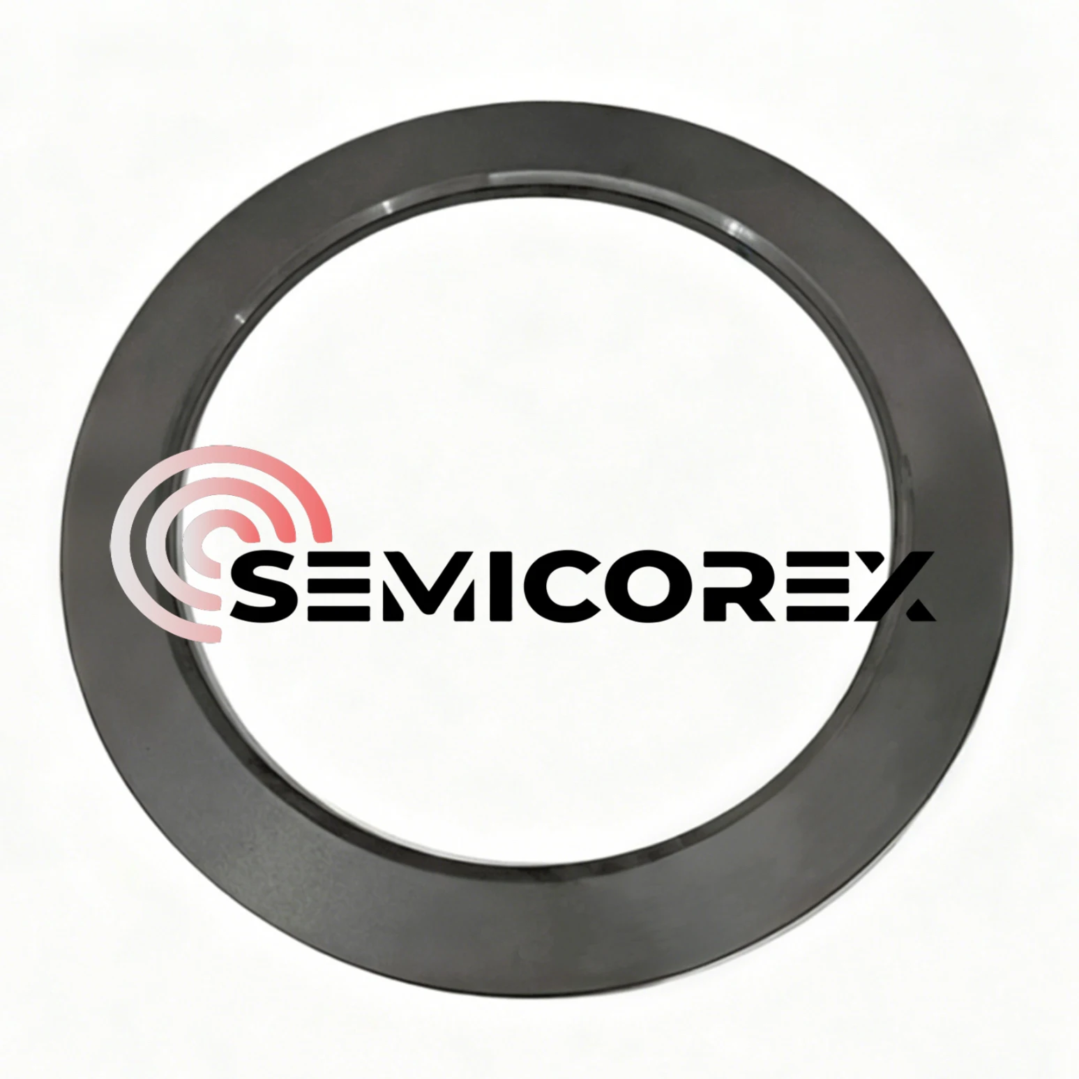
Why Focus Ring Is Indispensable for Etching Equipment?
Focus ring, also referred to as compensation ring or confinement ring, is an indispensable component of etching equipment, especially plasma dry etch equipment. Nanoscale precision etching processes in modern semiconductor manufacturing would not be achievable without it. The use of focus ring ensures etching uniformity, guarantees wafer surface etch rate, protects core hardware of the etch equipment, and ultimately improves semiconductor device yield and reduces production costs.
Core Functions of Focus Ring
1. Optimizes edge electric field and plasma distribution
Without a focus ring, electric field lines at the wafer edge become severely bent and divergent, resulting in the edge effect. This causes significant discrepancies in plasma density and ion bombardment energy between the wafer edge and the center region. The focus ring is arranged around the wafer to effectively elevate the wafer’s physical and electrical boundary and reshape the edge plasma distribution. It smooths the electric field profile at the wafer edge, much like turning a “steep cliff” into a “gentle slope.” This improvement creates a more uniform plasma sheath at the wafer edge, guiding ions to bombard the entire wafer surface at a more vertical and consistent angle, including the outermost dies.
2. Protects Electrostatic Chuck (ESC) and serves as a process chamber component
Plasma environments are highly corrosive. Without protection from the focus ring, high-energy plasma would directly bombard and etch the electrostatic chuck (ESC) that holds the wafer. Since ESCs are typically made of expensive materials such as alumina ceramic, their replacement cost is extremely high. The focus ring, as a replaceable consumable, acts as a sacrificial component to protect more critical equipment parts and reduce related costs. Focus rings are commonly made of silicon, quartz, silicon carbide, and other process-compatible materials. Particles generated from its erosion have a far smaller impact on the process than metallic contaminants (e.g., aluminum, sodium) released by eroded ESC materials. This effectively reduces the risk of chamber and wafer contamination by particles or reaction byproducts, thereby minimizing product defects.
3. Compensates for wafer thickness variations
The top surface of the focus ring is typically designed to be level with the wafer’s top surface. This ensures consistent spacing from the upper electrode to both the wafer surface and the focus ring surface, helping form a uniform electric field across the entire area and avoiding electric field distortion caused by height differences.
The focus ring is gradually etched thinner by plasma during processing. A thinned focus ring causes process s drift: as the focus ring height decreases due to erosion, its ability to confine the edge electric field weakens, and process performance at the wafer edge (e.g., etch rate, profile) gradually shifts. For this reason, the focus ring must be replaced periodically based on process throughput (e.g., accumulated RF hours).
Different etch processes (silicon etch, oxide etch, metal etch) may use focus rings made of different materials (e.g., monocrystalline silicon, quartz, silicon carbide, ceramic) to match etch rates and minimize contamination. In some advanced tools, advanced process control (APC) software tracks focus ring usage duration and may compensate for erosion effects by fine-tuning process parameters (e.g., power, pressure), extending service life while maintaining process stability.


