- English
- Español
- Português
- русский
- Français
- 日本語
- Deutsch
- tiếng Việt
- Italiano
- Nederlands
- ภาษาไทย
- Polski
- 한국어
- Svenska
- magyar
- Malay
- বাংলা ভাষার
- Dansk
- Suomi
- हिन्दी
- Pilipino
- Türkçe
- Gaeilge
- العربية
- Indonesia
- Norsk
- تمل
- český
- ελληνικά
- український
- Javanese
- فارسی
- தமிழ்
- తెలుగు
- नेपाली
- Burmese
- български
- ລາວ
- Latine
- Қазақша
- Euskal
- Azərbaycan
- Slovenský jazyk
- Македонски
- Lietuvos
- Eesti Keel
- Română
- Slovenski
- मराठी
- Srpski језик

What Roles Does the Annealing Process Play?
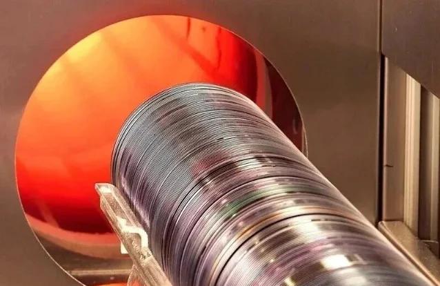
In wafer fabrication, annealing treatment is an indispensable processing step. Annealing is essentially a controlled heat treatment process, which involves heating silicon wafers to a specific temperature (typically between 600 °C and 1200 °C), holding them for a certain duration, and cooling them at an appropriate rate. It does not alter the macroscopic shape of wafers but repairs and optimizes their internal microstructures.
Functions of Annealing
By precisely regulating heating and cooling profiles, annealing process can activates dopant atoms, repairs lattice damage, relieves internal stress, and improves the electrical reliability of wafers. These critical performance enhancements lay a solid foundation for subsequent wafer processing, serving as a core prerequisite to ensure long-term stable operation of end-use semiconductor devices under high-power and high-integration scenarios.
1. Activation of Dopant Atoms
During ion implantation, high-energy dopant atoms (e.g., boron, phosphorus, arsenic) are driven into the silicon lattice like bullets. Most atoms get trapped in interstitial sites or random positions in an electrically inactive state-unable to supply free electrons or holes, and thus failing to modify silicon conductivity. Annealing supplies sufficient thermal energy to enable these interstitial atoms to migrate, occupy vacant lattice sites created by implantation damage, and integrate into the crystal lattice. This process is known as substitutional activation. Only activated dopants contribute free charge carriers to form PN junctions or conductive channels. Without annealing, implanted impurities merely exist physically within silicon with negligible impact on electrical performance.
2. Repair of Lattice Damage
The high-energy ion implantation displaces silicon atoms from lattice sites, generating numerous vacancies, interstitials, and even an amorphous layer several to tens of nanometers thick on the wafer surface. Such defective lattices suffer from low carrier mobility and severe leakage current. During annealing, thermal energy triggers vibration, diffusion, and rearrangement of silicon atoms. Amorphous regions recrystallize via solid-phase epitaxy to restore nearly perfect single-crystal structures, analogous to resurfacing a crater-pitted road to recover flatness and structural integrity.
3. Relief of Internal Stress
Thermal and mechanical stress accumulates in silicon wafers during high-temperature oxidation, thin-film deposition, and rapid temperature cycling. Unrelieved stress causes wafer bowing, slip lines, failed lithography focusing, or even device fracture. Through well-designed temperature profiles, annealing relaxes lattice atoms to uniformly release residual stress.
4. Improvement of Electrical ReliabilityCertain manufacturing steps introduce deep-level impurities such as heavy metals (iron, copper), which form recombination centers in the band gap, drastically reducing minority-carrier lifetime and increasing leakage current. High-temperature annealing drives these impurities to diffuse inward and be captured by surface gettering layers, purifying the active regions. This step is particularly critical for leakage-sensitive devices such as solar cells and detectors.
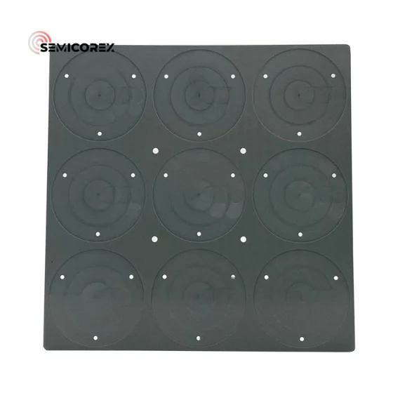
Semicorex offers high-quality RTP carriers in annealing process. If you have any inquiries or need additional details, please don't hesitate to get in touch with us.
Contact phone # +86-13567891907
Email: sales@semicorex.com