
- English
- Español
- Português
- русский
- Français
- 日本語
- Deutsch
- tiếng Việt
- Italiano
- Nederlands
- ภาษาไทย
- Polski
- 한국어
- Svenska
- magyar
- Malay
- বাংলা ভাষার
- Dansk
- Suomi
- हिन्दी
- Pilipino
- Türkçe
- Gaeilge
- العربية
- Indonesia
- Norsk
- تمل
- český
- ελληνικά
- український
- Javanese
- فارسی
- தமிழ்
- తెలుగు
- नेपाली
- Burmese
- български
- ລາວ
- Latine
- Қазақша
- Euskal
- Azərbaycan
- Slovenský jazyk
- Македонски
- Lietuvos
- Eesti Keel
- Română
- Slovenski
- मराठी
- Srpski језик

Why Are Porous Alumina Chucks Becoming the Preferred Choice for Precision Semiconductor Manufacturing
The semiconductor industry continues to demand higher precision, cleaner processing environments, and greater manufacturing efficiency. As wafer sizes increase and process tolerances become increasingly stringent, traditional wafer holding methods often struggle to meet modern production requirements. This is where Porous Alumina Chucks have emerged as a critical solution.
Manufactured using advanced porous ceramic technology, Porous Alumina Chucks provide uniform vacuum distribution, excellent thermal stability, superior chemical resistance, and outstanding dimensional accuracy. These characteristics make them indispensable in wafer processing, inspection, lithography, dicing, and other high-precision semiconductor applications.
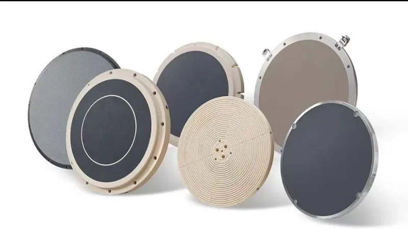
Table of Contents
- What Are Porous Alumina Chucks?
- How Do Porous Alumina Chucks Work?
- What Advantages Do Porous Alumina Chucks Offer?
- Why Is Alumina Ideal for Vacuum Chuck Applications?
- Where Are Porous Alumina Chucks Used?
- How Are Porous Alumina Chucks Manufactured?
- How Do They Compare with Traditional Chucks?
- How Should You Choose the Right Porous Alumina Chuck?
- Why Choose Semicorex?
- Frequently Asked Questions
What Are Porous Alumina Chucks?
Porous Alumina Chucks are advanced ceramic vacuum chucks designed to securely hold delicate substrates, wafers, glass panels, and electronic components during manufacturing processes. Unlike conventional vacuum chucks that rely on grooves or drilled holes, these chucks contain a network of interconnected microscopic pores throughout the ceramic structure.
The porous structure allows vacuum pressure to be distributed evenly across the entire surface, creating highly uniform holding force while minimizing localized stress points. This significantly reduces the risk of wafer deformation, breakage, or particle contamination.
Because of their unique structure, Porous Alumina Chucks are widely used in semiconductor production where ultra-high precision and cleanliness are essential.
How Do Porous Alumina Chucks Work?
The working principle of Porous Alumina Chucks is relatively straightforward yet highly effective.
When vacuum is applied to the backside of the chuck, air is drawn through the interconnected pores within the ceramic body. This creates a uniform suction force across the entire contact surface.
Unlike conventional vacuum systems that generate concentrated suction at discrete holes, the porous design provides:
- Even vacuum distribution
- Stable wafer positioning
- Reduced mechanical stress
- Improved flatness control
- Enhanced process consistency
This uniform holding mechanism is especially valuable when processing ultra-thin wafers or fragile substrates used in advanced semiconductor manufacturing.
What Advantages Do Porous Alumina Chucks Offer?
The popularity of Porous Alumina Chucks continues to grow because they provide numerous advantages over traditional holding technologies.
Uniform Vacuum Distribution
The porous ceramic structure eliminates uneven suction zones, ensuring stable substrate positioning throughout the manufacturing process.
Excellent Thermal Stability
Alumina ceramics maintain dimensional stability across a wide temperature range, making them suitable for high-temperature processing environments.
Outstanding Chemical Resistance
Porous Alumina Chucks resist acids, alkalis, solvents, and aggressive process chemicals commonly found in semiconductor fabrication facilities.
Particle Reduction
The absence of mechanical clamping mechanisms reduces particle generation and contamination risks.
Long Service Life
High hardness and wear resistance contribute to extended operational lifespan and reduced maintenance costs.
Why Is Alumina Ideal for Vacuum Chuck Applications?
Alumina ceramic has become one of the most widely used engineering ceramics due to its exceptional combination of physical, thermal, and chemical properties.
| Property | Benefit for Vacuum Chucks |
|---|---|
| High Hardness | Excellent wear resistance and durability |
| Thermal Stability | Maintains dimensional accuracy at elevated temperatures |
| Chemical Resistance | Compatible with harsh semiconductor chemicals |
| Electrical Insulation | Suitable for sensitive electronic manufacturing |
| Low Thermal Expansion | Improves process precision |
| Porous Structure Control | Enables uniform vacuum distribution |
These characteristics make alumina an ideal material for precision vacuum chuck applications where reliability and performance are critical.
Where Are Porous Alumina Chucks Used?
Porous Alumina Chucks are utilized across multiple high-tech industries.
Semiconductor Manufacturing
- Wafer handling
- Wafer inspection
- Lithography systems
- CMP processing
- Etching operations
LED Manufacturing
LED substrates require precise positioning and minimal contamination, making Porous Alumina Chucks an ideal solution.
MEMS Production
Microelectromechanical systems involve highly delicate structures that benefit from uniform vacuum support.
Display Panel Manufacturing
Flat panel displays and OLED production lines frequently utilize porous ceramic vacuum technologies.
Precision Electronics Assembly
Electronic components often require stable positioning during bonding, inspection, and testing processes.
How Are Porous Alumina Chucks Manufactured?
Producing high-performance Porous Alumina Chucks requires advanced ceramic engineering expertise and strict quality control.
The manufacturing process generally includes:
- High-purity alumina powder preparation
- Controlled pore-forming material blending
- Precision shaping and forming
- High-temperature sintering
- Pore structure optimization
- Precision machining
- Surface finishing
- Inspection and testing
Every stage directly affects pore uniformity, permeability, dimensional accuracy, and overall performance.
Leading manufacturers such as Semicorex employ sophisticated production technologies to ensure consistent quality and repeatable performance.
How Do They Compare with Traditional Chucks?
| Feature | Porous Alumina Chucks | Traditional Vacuum Chucks |
|---|---|---|
| Vacuum Distribution | Uniform | Localized |
| Wafer Protection | Excellent | Moderate |
| Particle Generation | Low | Higher |
| Precision | Very High | Moderate |
| Maintenance | Lower | Higher |
| Suitability for Thin Wafers | Excellent | Limited |
This comparison highlights why more semiconductor manufacturers are transitioning to Porous Alumina Chucks for critical production processes.
How Should You Choose the Right Porous Alumina Chuck?
Selecting the optimal Porous Alumina Chuck requires evaluating several important factors.
Substrate Size
The chuck must match the dimensions and geometry of the workpiece.
Porosity Level
Different applications require different airflow and vacuum characteristics.
Surface Flatness
High-precision manufacturing demands exceptional flatness and dimensional accuracy.
Operating Environment
Temperature, chemical exposure, and process conditions should be carefully considered.
Vacuum Requirements
Holding force requirements vary based on substrate weight and process parameters.
Working with experienced suppliers ensures the selected solution meets both current and future production needs.
Why Choose Semicorex?
As semiconductor manufacturing technology continues to advance, the demand for reliable ceramic components becomes increasingly important. Semicorex has established itself as a trusted supplier of advanced semiconductor process materials and precision ceramic solutions.
Semicorex provides high-quality Porous Alumina Chucks designed to meet the rigorous requirements of modern semiconductor fabrication facilities. Through continuous innovation, strict quality control, and extensive industry expertise, the company delivers products that support improved process stability, higher yields, and long-term operational reliability.
Key advantages include:
- High-purity alumina materials
- Consistent pore distribution
- Precision machining capabilities
- Excellent dimensional accuracy
- Customized design support
- Reliable global supply chain
- Professional technical assistance
These strengths make Semicorex a preferred partner for semiconductor manufacturers worldwide.
Frequently Asked Questions
What is the primary purpose of Porous Alumina Chucks?
Their primary purpose is to securely hold wafers and substrates through uniform vacuum distribution while minimizing mechanical stress and contamination.
Are Porous Alumina Chucks suitable for thin wafer processing?
Yes. Their evenly distributed vacuum force makes them ideal for handling ultra-thin and fragile wafers.
How long do Porous Alumina Chucks typically last?
Service life depends on operating conditions, but high-quality alumina ceramics generally offer excellent durability and long-term performance.
Can Porous Alumina Chucks withstand harsh chemicals?
Yes. Alumina ceramics provide strong resistance to many chemicals commonly used in semiconductor manufacturing.
Are custom designs available?
Many manufacturers, including Semicorex, offer customized Porous Alumina Chucks tailored to specific equipment and process requirements.
Why are Porous Alumina Chucks becoming increasingly popular?
Because they provide superior precision, reduced contamination, improved wafer protection, and better process consistency compared with traditional vacuum chuck technologies.
Conclusion
As semiconductor devices become smaller, more complex, and more performance-driven, manufacturing equipment must evolve to meet increasingly demanding process requirements. Porous Alumina Chucks have proven to be one of the most effective solutions for achieving precise wafer handling, superior vacuum uniformity, contamination control, and long-term reliability.
Whether you are upgrading existing semiconductor equipment or developing next-generation manufacturing systems, investing in high-quality Porous Alumina Chucks can significantly enhance productivity, yield, and process stability. If you are looking for advanced ceramic solutions backed by industry expertise and proven performance, Semicorex is ready to help. Contact us today to discuss your specific application requirements and discover how our Porous Alumina Chucks can support your manufacturing success.


