- English
- Español
- Português
- русский
- Français
- 日本語
- Deutsch
- tiếng Việt
- Italiano
- Nederlands
- ภาษาไทย
- Polski
- 한국어
- Svenska
- magyar
- Malay
- বাংলা ভাষার
- Dansk
- Suomi
- हिन्दी
- Pilipino
- Türkçe
- Gaeilge
- العربية
- Indonesia
- Norsk
- تمل
- český
- ελληνικά
- український
- Javanese
- فارسی
- தமிழ்
- తెలుగు
- नेपाली
- Burmese
- български
- ລາວ
- Latine
- Қазақша
- Euskal
- Azərbaycan
- Slovenský jazyk
- Македонски
- Lietuvos
- Eesti Keel
- Română
- Slovenski
- मराठी
- Srpski језик

Brief Introduction to SiC Wafer Fabrication Process
As the indispensable substrate material in the cutting-edge semiconductor industry, silicon carbide wafers exhibit excellent thermal and electrical properties, boasting broad application prospects in high-temperature, high-frequency, high-power and radiation-resistant integrated electronic devices.
Since the machining precision of SiC substrates directly impacts the performance of final semiconductor devices, extremely stringent requirements are imposed on the surface quality of SiC wafers for semiconductor manufacturing applications. This paper briefly describes the manufacturing process of high-quality silicon carbide wafers.
1. Raw Material Preparation
High-purity silicon powder and carbon powder, mixed in a specific ratio, are reacted at a temperature exceeding 2000℃ to synthesize silicon carbide particles. And then the high-quality silicon carbide micro-powder that fully meets the requirements for SiC crystal growth undergoes subsequent refining procedures like crushing and chemical cleaning.
2. Crystal Growth
High-quality SiC micro-powder is placed in the crucible within a high-temperature furnace and then heated to its sublimation temperature, in which ist decomposes into gases like Si, Si₂C and SiC₂. Under the effect of an axial temperature gradient, these gases migrate upward to the upper furnace zone and deposit around the SiC seed crystal, gradually growing into a cylindrical ingot.

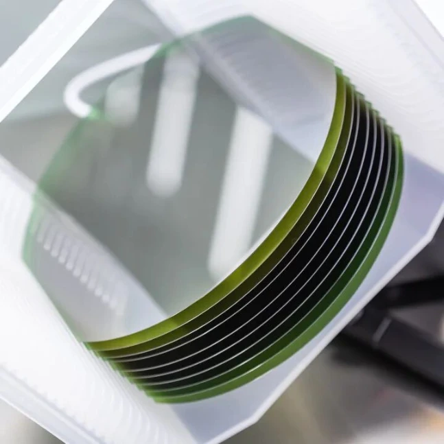
3. Ingot Processing & Wafer Slicing
The as-grown silicon carbide ingot is oriented by an X-ray single crystal orientation instrument and processed into standard-diameter blanks through surface flattening and cylindrical grinding. The finished standard SiC blanks are then sliced into thin wafers with a thickness of no more than 1 mm by multi-wire slicing equipment.

4. Wafer Lapping & Polishing
Sliced wafers are ground by using diamond lapping slurries of various particle sizes to achieve the required flatness and roughness, combined mechanical polishing and chemical mechanical polishing processes are applied to obtain the damage-free ultra-smooth surface of SiC wafers.
5. Wafer Inspection
Various parameters of SiC wafers are tested by professional instruments, including optical microscope, X-ray diffractometer, atomic force microscope, non-contact resistivity tester, surface flatness tester, and comprehensive surface defect tester. The tested items include micropipe density, crystal quality, surface roughness, resistivity, warp, bow, thickness variation, and surface scratches, based on which the quality grade of each wafer is classified.
6. Wafer Cleaning
Polished SiC wafers are typically cleaned using chemical cleaning agents and ultra-pure water to thoroughly remove the unwanted surface contaminants and residual polishing slurry and then dried in an ultra-high purity nitrogen atmosphere with spin dryers. The cleaned and dried wafers are packaged into clean wafer cassettes in the semiconductor-grade cleanroom, making them fully meet the downstream cleanliness standards.