
- English
- Español
- Português
- русский
- Français
- 日本語
- Deutsch
- tiếng Việt
- Italiano
- Nederlands
- ภาษาไทย
- Polski
- 한국어
- Svenska
- magyar
- Malay
- বাংলা ভাষার
- Dansk
- Suomi
- हिन्दी
- Pilipino
- Türkçe
- Gaeilge
- العربية
- Indonesia
- Norsk
- تمل
- český
- ελληνικά
- український
- Javanese
- فارسی
- தமிழ்
- తెలుగు
- नेपाली
- Burmese
- български
- ລາວ
- Latine
- Қазақша
- Euskal
- Azərbaycan
- Slovenský jazyk
- Македонски
- Lietuvos
- Eesti Keel
- Română
- Slovenski
- मराठी
- Srpski језик

Semiconductor etching process technology
Etching, or etching, is a crucial step in semiconductor manufacturing, microelectronics IC manufacturing, and micro/nano manufacturing processes. It's a primary patterning process associated with photolithography. In a narrow sense, etching is essentially photolithographic etching, where photoresist is first exposed using photolithography, and then other methods are used to etch away the unwanted material. Etching is the process of selectively removing unwanted material from the surface of a silicon wafer using chemical or physical methods. Its basic goal is to accurately replicate the mask pattern on the coated silicon wafer. With the development of microfabrication processes, etching has broadly become a general term for the stripping and removal of material using solutions, reactive ions, or other mechanical methods, becoming a common term in microfabrication.
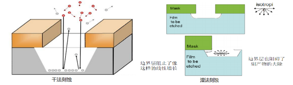
Etching can be broadly categorized into two types: wet etching and dry etching. In dry etching, the gas is excited at high frequencies (primarily 13.56 MHz or 2.45 GHz). Under pressures of 1 to 100 Pa, its mean free path ranges from a few millimeters to a few centimeters. There are three main types of dry etching:
• Physical dry etching: Accelerates the physical wear of particles on the wafer surface;
• Chemical dry etching: The gas reacts chemically with the wafer surface;
• Chemical-physical dry etching: A physical etching process with chemical properties;
1. Ion beam etching
Ion beam etching is a physical dry etching process. Argon ions are radiated onto the surface in an ion beam of approximately 1 to 3 keV. Due to the energy of the ions, they bombard the surface material. The wafer is inserted vertically or at an angle into the ion beam, and the etching process is absolutely anisotropic. Selectivity is low because it does not differentiate between layers. The gas and the polished material are expelled by a vacuum pump; however, because the reaction products are not gaseous, particles can deposit on the wafer or chamber walls.
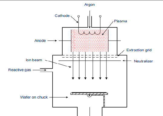
To avoid these particles, a second gas is introduced into the chamber. This gas reacts with argon ions, inducing a physicochemical etching process. Some of the gas reacts with the surface, but some reacts with the polished particles to form gaseous byproducts. Almost all materials can be etched using this method. Due to vertical radiation, wear on the vertical walls is very low (high anisotropy). However, due to low selectivity and low etching rate, this process is rarely used in modern semiconductor manufacturing.
2. Plasma Etching
Plasma etching is an absolutely chemical etching process (chemical dry etch). Its advantage is that the wafer surface is not damaged by accelerated ions. Due to the movable particles of the etching gas, the etching profile is isotropic, making this method suitable for removing entire film layers (e.g., back-side cleaning after thermal oxidation).
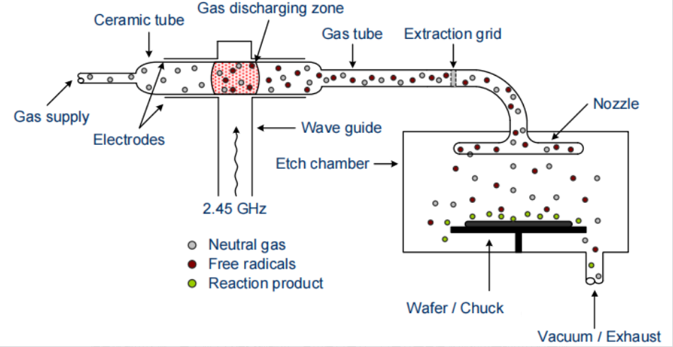
One type of reactor used for plasma etching is a downstream reactor. The plasma is ignited at a high frequency of 2.45 GHz through impact ionization, and the impact ionization site separates from the wafer.
In the gas discharge region, various particles, including free radicals, are present due to the impact. Free radicals are neutral atoms or molecules with unsaturated electrons and are therefore highly reactive. As a neutral gas, tetrafluoromethane (CF4) is introduced into the gas discharge region and separates into CF2 and fluorine molecules (F2). Similarly, fluorine can be separated from CF4 by adding oxygen (O2):
2 CF4 + O2 ---> 2 COF2 + 2 F2
The fluorine molecule can be split into two separate fluorine atoms by the energy in the gas discharge region: each fluorine atom is a fluorine free radical, as each atom has seven valence electrons and aims to achieve an inert gas configuration. In addition to the neutral free radicals, there are several partially charged particles (CF+4, CF+3, CF+2, ...). All particles, free radicals, etc., then enter the etching chamber through a ceramic tube. Charged particles can be blocked from the etching chamber by an extraction grating or recombine during their formation of neutral molecules. Fluorine radicals also partially recombine, but enough to reach the etching chamber, react on the wafer surface, and cause chemical abrasion. Other neutral particles are not part of the etching process and are depleted along with the reaction products.
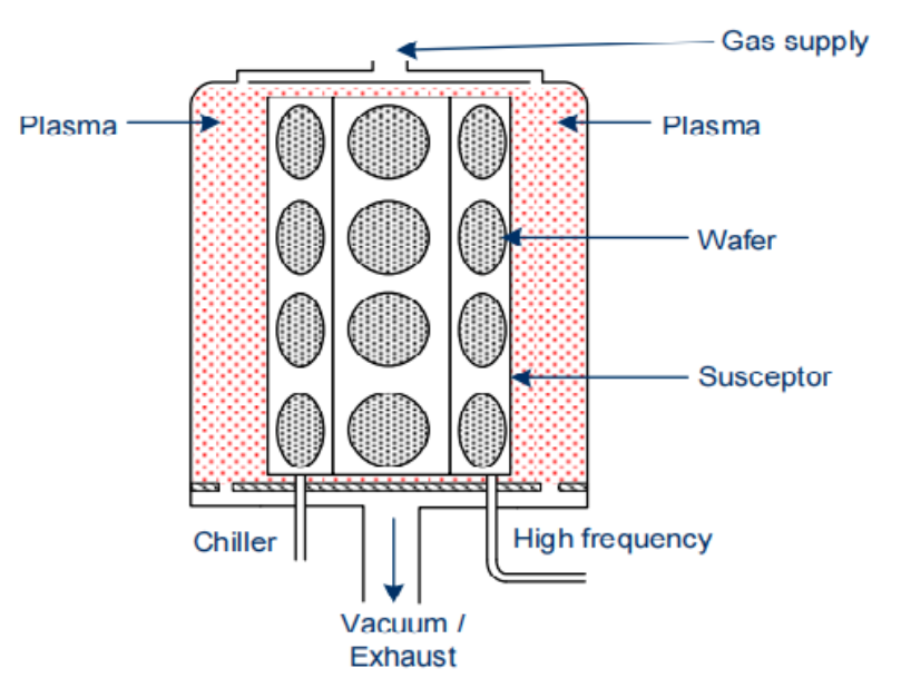
Examples of thin films that can be etched in plasma etching: • Silicon: Si + 4F ---> SiF4 • Silicon dioxide: SiO2 + 4F ---> SiF4 + O2 • Silicon nitride: Si3N4 + 12F ---> 3SiF4 + 2N2 3. Reactive ion etching (RIE) characteristics: Selectivity, etching profile, etching rate, uniformity, and repeatability can all be controlled very precisely in reactive ion etching. Isotropic etching profiles as well as anisotropic ones are possible. Therefore, RIE is a chemical physical etching process and is the most important process in semiconductor manufacturing for constructing a wide variety of thin films. In the process chamber, the wafer is placed on a high-frequency electrode (HF electrode). Plasma is generated by impact ionization, in which free electrons and positively charged ions appear. If the HF electrode is at a positive voltage, free electrons accumulate on it and cannot leave the electrode again due to their electron affinity. Therefore, the electrode is charged to -1000 V (bias voltage). Slow ions that cannot follow the rapidly alternating field move towards the negatively charged electrode.
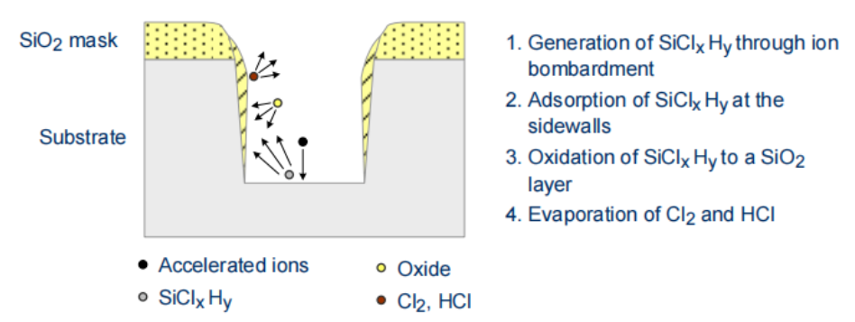
If the mean free path of the ions is high, the particles bombard the wafer surface at almost perpendicular angles. Thus, the material is ejected from the surface by accelerated ions (physical etching), and some particles also chemically react with the surface. Lateral sidewalls are unaffected, so there is no wear and the etch profile remains anisotropic. The selectivity is not too small, but it is not too large due to the physical etching process. Furthermore, the wafer surface is damaged by accelerated ions and must be cured by thermal annealing. The chemical part of the etching process is accomplished through the reaction of free radicals with the surface and the material being physically milled, so it does not redeposit onto the wafer or chamber walls as in ion beam etching. By increasing the pressure in the etching chamber, the mean free path of the particles decreases. Therefore, there are more collisions, and the particles travel in different directions. This results in less directional etching, and the etching process acquires more chemical properties. Increased selectivity results in a more isotropic etch profile. Anisotropic etch profiles are achieved through passivation of the sidewalls during silicon etching. Oxygen in the etching chamber reacts with the milled silicon to form silicon dioxide, which is deposited on the vertical sidewalls. The oxide film on the horizontal regions is removed due to ion bombardment, allowing the lateral etching process to continue.
The etch rate depends on pressure, high-frequency generator power, process gas, actual gas flow rate, and wafer temperature. Anisotropy increases with increasing high-frequency power, decreasing pressure, and decreasing temperature. The uniformity of the etching process depends on the gas, the distance between the two electrodes, and the electrode material. If the distance is too small, the plasma cannot be dispersed uniformly, resulting in inhomogeneity. Increasing the electrode distance reduces the etch rate because the plasma is distributed over an expanded volume. For electrodes, carbon has proven to be the preferred material. Because fluorine and chlorine also attack carbon, the electrodes produce a uniform strained plasma, thus the wafer edges are affected in the same way as the wafer center.
Selectivity and etch rate depend heavily on the process gas. For silicon and silicon compounds, fluorine and chlorine are primarily used.
Etching processes are not limited to a single gas, gas mixture, or fixed process parameters. For example, native oxides on polysilicon can be removed first at a high etch rate and with low selectivity, followed by etching of the polysilicon with higher selectivity relative to the underlying layers.
Semicorex offers various SiC components in etching process. If you have any inquiries or need additional details, please don't hesitate to get in touch with us.
Contact phone # +86-13567891907
Email: sales@semicorex.com


