- English
- Español
- Português
- русский
- Français
- 日本語
- Deutsch
- tiếng Việt
- Italiano
- Nederlands
- ภาษาไทย
- Polski
- 한국어
- Svenska
- magyar
- Malay
- বাংলা ভাষার
- Dansk
- Suomi
- हिन्दी
- Pilipino
- Türkçe
- Gaeilge
- العربية
- Indonesia
- Norsk
- تمل
- český
- ελληνικά
- український
- Javanese
- فارسی
- தமிழ்
- తెలుగు
- नेपाली
- Burmese
- български
- ລາວ
- Latine
- Қазақша
- Euskal
- Azərbaycan
- Slovenský jazyk
- Македонски
- Lietuvos
- Eesti Keel
- Română
- Slovenski
- मराठी
- Srpski језик
How Alumina Ceramic Chucks Eliminate Static Electricity and Contamination During Wafer Etching?
Alumina ceramic chucks are precision ceramic wafer holding components sintered from ultra-high-purity alumina powder. Their core function is to firmly adsorb and accurately position wafers of various sizes throughout semiconductor manufacturing processes. During precision dry etching of wafers, the chuck surface makes direct contact with the wafer backside. Accordingly, the raw material purity, physicochemical properties and surface structural design of the chuck directly affect etching uniformity and wafer surface yield, exerting a decisive impact on the final quality of processed chips.
Wafer etching processes present two severe challenges: high risks of electrostatic adhesion and particulate contamination. To tackle these two critical industry issues, alumina ceramic chucks leverage material modification processes, optimized microstructural design, and the outstanding comprehensive physicochemical properties of ceramics to fundamentally suppress static charge accumulation and particle contamination, complying with the stringent production standards for front-end high-end semiconductor etching.
1. Solutions to Electrostatic Adhesion Risks
Conventional pure alumina ceramics are excellent insulators. However, in the high-energy plasma environment of etching processes, large volumes of static charges readily accumulate on insulator surfaces, resulting in overly strong residual adhesion that locks wafers firmly in place, or even electrostatic breakdown. To address this problem, advanced alumina ceramic chucks adopt the following semi-conductive modification technologies:
A. Semi-conductive modification
Trace transition metal oxides such as titanium dioxide (TiO₂) and chromium sesquioxide (Cr₂O₃) are doped into the alumina matrix to precisely tune its bulk resistivity within the static dissipative range.
B. Johnsen-Rahbek (J-R) effect utilization
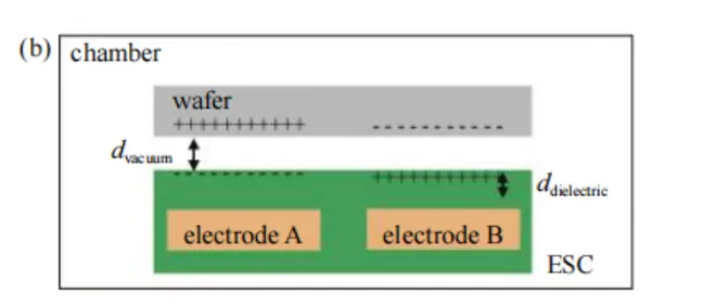
Modified semi-conductive alumina ceramic chucks generate clamping force mainly via the J-R effect. When voltage is applied, micro-charges migrate to micro-protrusions on the ceramic surface, forming an ultra-thin charge layer between the wafer and chuck. This delivers clamping force several times stronger than traditional Coulomb force with an ultra-fast response speed. Once power is cut off, accumulated static charges dissipate rapidly through semi-conductive pathways, completely eliminating wafer release delay and residual static electricity issues.
2. Solutions to Particulate Contamination Problems
Etching processes, especially dry plasma etching, employ highly corrosive gases (CF₄, CHF₃, Cl₂, etc.) accompanied by high-energy ion bombardment. Chucks lacking sufficient wear and corrosion resistance will erode and shed contaminative particles. Alumina ceramics achieve near-zero contamination through multi-dimensional optimized processes:
A. Ultra-high-purity substrate
For front-end semiconductor applications, alumina chucks restrict metallic impurities including copper (Cu), iron (Fe), sodium (Na) and potassium (K) to extremely low ppm or even ppb levels. This prevents metal ion migration onto wafers caused by material abrasion during etching, which would otherwise trigger irreversible circuit short-circuiting and device failure.
B. Superior resistance to plasma bombardment
High-purity alumina ceramics feature exceptional chemical stability and high lattice energy. Under continuous bombardment by fluorine-based and chlorine-based plasma, they maintain an ultra-low erosion rate and resist particle shedding effectively.
C. Precision surface treatment and micro-pillar design
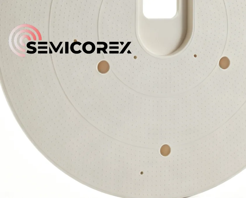
The chuck surface undergoes nano-scale ultra-precision polishing. More importantly, full-area contact between the chuck and wafer is avoided by arranging countless tiny micro-pillars on the surface, cutting the contact area by over 90%. This drastically reduces particles generated by mechanical friction. Even trace particulates will fall into the grooves between micro-pillars and never adhere to the wafer backside.