- English
- Español
- Português
- русский
- Français
- 日本語
- Deutsch
- tiếng Việt
- Italiano
- Nederlands
- ภาษาไทย
- Polski
- 한국어
- Svenska
- magyar
- Malay
- বাংলা ভাষার
- Dansk
- Suomi
- हिन्दी
- Pilipino
- Türkçe
- Gaeilge
- العربية
- Indonesia
- Norsk
- تمل
- český
- ελληνικά
- український
- Javanese
- فارسی
- தமிழ்
- తెలుగు
- नेपाली
- Burmese
- български
- ລາວ
- Latine
- Қазақша
- Euskal
- Azərbaycan
- Slovenský jazyk
- Македонски
- Lietuvos
- Eesti Keel
- Română
- Slovenski
- मराठी
- Srpski језик
Brief Introduction of Rapid Thermal Annealing
Rapid thermal annealing (abbreviated as RTA or RTP) is a rapid thermal processing technology in semiconductor manufacturing. Its core principle is to rapidly heat the wafer surface using a high-intensity radiant heat source (such as halogen lamps, lasers, flash lamps, etc.), heating the wafer to the target high temperature in an extremely short time (seconds or milliseconds), followed by a rapid cooling process.
Main types of annealing processes
Driven by the demand for ever-shorter annealing durations in advanced manufacturing nodes, a full portfolio of annealing technologies has been developed, with processing time scaled down sequentially from seconds to milliseconds, and further to microseconds.
1. Soak rapid thermal annealing
Traditional RTA process with 1 ~ 30 seconds dwell at peak temperature.
2. Spike rapid thermal annealing
Wafers reach peak temperature (~1050°C) with negligible sub-second dwell before immediate cooling; the mainstream process for ultra-shallow junction formation.
3. Flash lamp annealing
Intense millisecond-scale flash from arc lamps instantaneously heats only the wafer surface while keeping the bulk substrate cool.
4.Laser spike annealing
The scanning laser beam delivers microsecond-to-millisecond localized heating limited to the topmost silicon layer. It delivers the lowest thermal budget, highest dopant activation efficiency and the shallowest possible junctions.
Why is rapid thermal annealing required after ion implantation?
Ion implantation is an aggressive bombardment process that relies on high-energy ions to strike silicon wafers to complete doping, which will cause serious damage to the wafer and result in two critical defects that can only be resolved via the annealing process.
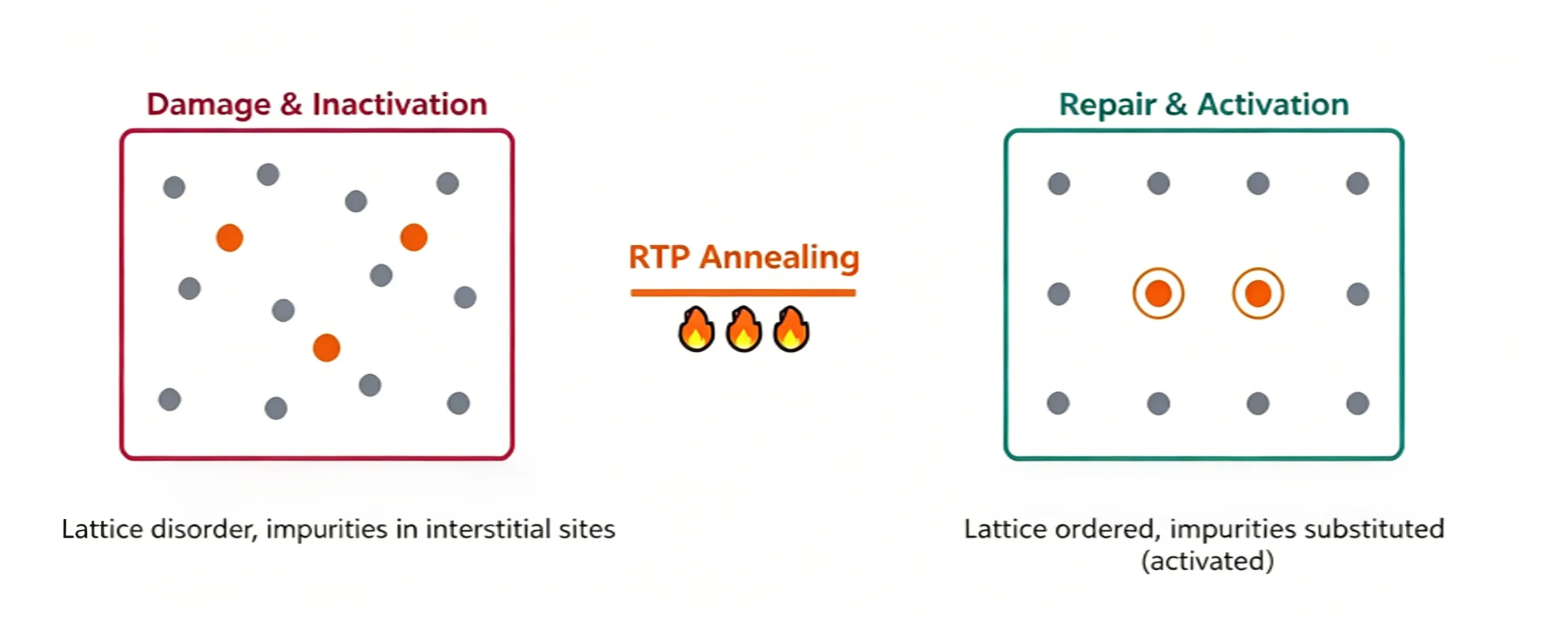
1. Dopants occupy improper lattice sites
For dopant atoms (Boron, Phosphorus, Arsenic) to generate free charge carriers (holes or electrons), they must occupy substitutional lattice sites, replacing native silicon atoms. Immediately after implantation, however, most dopants get trapped at interstitial positions. These interstitial dopants are electrically inactive and cannot contribute any carriers to conduction. Annealing provides thermal energy to drive interstitial dopants to migrate to substitutional sites, thus achieving true “dopant activation” and turning them into functional donors or acceptors. The dopant activation rate directly governs the sheet resistance of the doped layer.
2. Lattice structure is severely damaged
High-dose ion implantation disrupts the ordered crystal lattice on the wafer surface and may even lead to amorphization: the originally well-aligned single-crystal silicon transforms into a disordered glass-like amorphous silicon layer. Annealing allows this amorphous silicon layer to be grown back into a single crystal using the intact underlying silicon as a template. This process is called solid-phase epitaxial recrystallization (SPER).
Why must the annealing process be "rapid"?
If high-temperature treatment is mandatory, why not use conventional furnaces for prolonged heating instead of rapid thermal annealing processing? The reason is that high temperatures not only activate impurities but also cause them to diffuse inward, making the junction deeper. Advanced semiconductor devices require ultra-shallow junctions (USJ), the shallower the junction, the better.
Dopant diffusion distance is determined by the thermal budget, defined by the formula:
Diffusion Length ≈ √(D · t), D ∝ exp(−Eₐ/kT)
D = dopant diffusion coefficient (rises exponentially with temperature)
t = dwell time at high temperature
Higher temperatures and longer thermal dwell times both lead to deeper junctions, creating a fundamental tradeoff: sufficient high temperature is necessary for full dopant activation, yet minimal heating duration is required to suppress junction deepening.
The only viable solution is fast ramping to peak temperature followed by immediate cooling, limiting high-temperature exposure to an ultra-short window. This is the core advantage of rapid thermal annealing over conventional furnace heating treatment: second or even millisecond-scale temperature cycling minimizes the overall thermal budget.
Semicorex offers high-quality RTP/RTA wafer carriers based on customers’ needs. If you have any inquiries or need additional details, please don't hesitate to get in touch with us.
Contact phone # +86-13567891907
Email: sales@semicorex.com