
- English
- Español
- Português
- русский
- Français
- 日本語
- Deutsch
- tiếng Việt
- Italiano
- Nederlands
- ภาษาไทย
- Polski
- 한국어
- Svenska
- magyar
- Malay
- বাংলা ভাষার
- Dansk
- Suomi
- हिन्दी
- Pilipino
- Türkçe
- Gaeilge
- العربية
- Indonesia
- Norsk
- تمل
- český
- ελληνικά
- український
- Javanese
- فارسی
- தமிழ்
- తెలుగు
- नेपाली
- Burmese
- български
- ລາວ
- Latine
- Қазақша
- Euskal
- Azərbaycan
- Slovenský jazyk
- Македонски
- Lietuvos
- Eesti Keel
- Română
- Slovenski
- मराठी
- Srpski језик

Released 850V High Power GaN HEMT Epitaxial Products
In November 2023, Semicorex released 850V GaN-on-Si epitaxial products for high-voltage, high-current HEMT power device applications. Compared to other substrates for HMET power devices, GaN-on-Si enables larger wafer sizes and more diversified applications, and it can also be quickly introduced into the mainstream silicon chip process in fabs, which is a unique advantage for improving the yield of power devices.
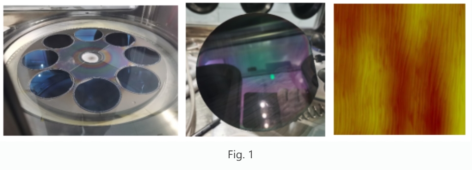
Traditional GaN power devices, because of its maximum voltage generally stay in the low-voltage application stage, the application field is relatively narrow, limiting the growth of the GaN application market. For high-voltage GaN-on-Si products, due to GaN epitaxy is a heterogeneous epitaxial process, epitaxial process there are such as: lattice mismatch, expansion coefficient mismatch, high dislocation density, low crystallization quality and other difficult problems, so epitaxial growth of high-voltage HMET epitaxial products is very challenging. Semicorex has achieved high uniformity of the epitaxial wafer by improving the growth mechanism and precisely controlling the growth conditions, high breakdown voltage and low leakage current of the epitaxial wafer by utilizing the unique buffer layer growth technology, and excellent 2D electron gas concentration by precisely controlling the growth conditions. As a result, we have successfully overcome the challenges posed by GaN-on-Si heterogeneous epitaxial growth and successfully developed products suitable for high voltage (Fig. 1).
Specifically:
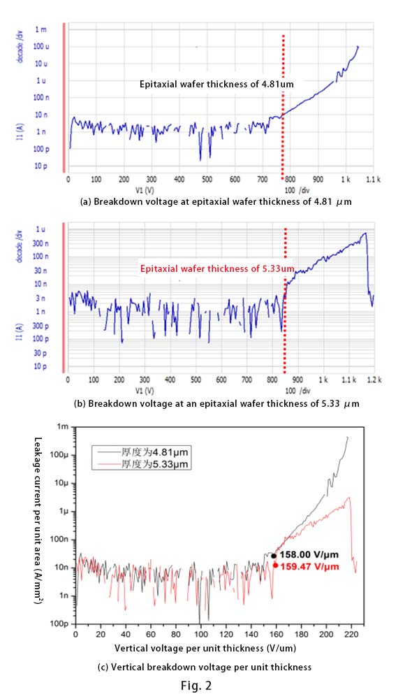
● True high-voltage resistance. In terms of voltage withstanding, we have truly achieved in the industry to maintain a low leakage current under 850V voltage conditions (Fig. 2), which ensures the safe and stable operation of HEMT device products over the voltage range of 0-850V, and is one of the leading products in the domestic market. By utilizing Semicorex's GaN-on-Si epitaxial wafers, 650V, 900V, and 1200V HEMT products can be developed, driving GaN to higher voltage and higher power applications.
●The world's top level of voltage withstand control level. Through the improvement of key technologies, a safe working voltage of 850V can be realized with an epitaxial layer thickness of only 5.33μm, and a vertical breakdown voltage of 158V/μm per unit thickness, with an error of less than 1.5V/μm, i.e., an error of less than 1% (Fig. 2(c)), which is the world's top level.
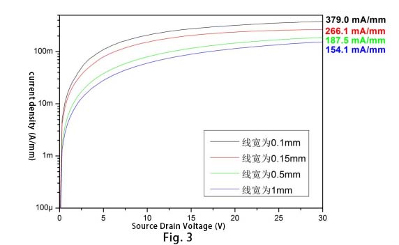
●The first company in China to realize GaN-on-Si epitaxial products with current density greater than 100mA/mm. higher current density is suitable for high power applications. Smaller chip, smaller module size, and less thermal effect can greatly reduce the module cost. Suitable for applications requiring higher power and higher on-state current, such as power grids (Figure 3).
●The cost is reduced by 70%, compared with the same type of products in China. Semicorex firstly, through the industry's best unit thickness performance enhancement technology, to greatly reduce the epitaxial growth time and material costs, so that the cost of GaN-on-Si epitaxial wafers tends to be closer to the range of the existing silicon device epitaxial, which can significantly reduce the cost of gallium nitride devices, and promote the application range of gallium nitride devices towards deeper and deeper. The application scope of GaN-on-Si devices will be developed in a deeper and wider direction.
Previous:What is C/C composite?


