
- English
- Español
- Português
- русский
- Français
- 日本語
- Deutsch
- tiếng Việt
- Italiano
- Nederlands
- ภาษาไทย
- Polski
- 한국어
- Svenska
- magyar
- Malay
- বাংলা ভাষার
- Dansk
- Suomi
- हिन्दी
- Pilipino
- Türkçe
- Gaeilge
- العربية
- Indonesia
- Norsk
- تمل
- český
- ελληνικά
- український
- Javanese
- فارسی
- தமிழ்
- తెలుగు
- नेपाली
- Burmese
- български
- ລາວ
- Latine
- Қазақша
- Euskal
- Azərbaycan
- Slovenský jazyk
- Македонски
- Lietuvos
- Eesti Keel
- Română
- Slovenski
- मराठी
- Srpski језик

Mainstream Debonding Methods
With the advancement of semiconductor processing and rising demand for electronic components, the application of ultra-thin wafers (thickness less than 100 micrometers) has become increasingly critical. However, with ongoing reductions in wafer thickness, wafers are highly vulnerable to breakage during subsequent processes, such as grinding, etching, and metallization.
Temporary bonding and debonding technologies are typically applied to guarantee the stable performance and production yield of semiconductor devices. The ultra-thin wafer is temporarily fixed onto a rigid carrier substrate, and after backside processing, the two are separated. This separation process is known as debonding, which primarily includes thermal debonding, laser debonding, chemical debonding, and mechanical debonding.
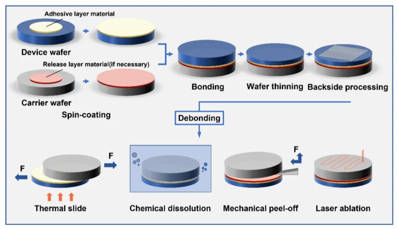
Thermal Debonding
Thermal debonding is a method that separates ultra-thin wafers from carrier substrates by heating to soften and decompose the bonding adhesive, thereby losing its adhesiveness. It is mainly divided into thermal slide debonding and thermal decomposition debonding.
Thermal slide debonding usually involves heating bonded wafers to their softening temperature, which ranges approximately from 190°C to 220°C. At this temperature, the bonding adhesive loses its adhesiveness, and ultra-thin wafers can be slowly pushed or peeled off carrier substrates by the shearing force applied by devices such as vacuum chucks to achieve a smooth separation. While in the thermal decomposition debonding, bonded wafers are heated to a higher temperature, causing chemical decomposition (molecular chain scission) of the adhesive and completely losing its adhesion. As a result, bonded wafers can be detached naturally without any mechanical force.
Laser debonding
Laser debonding is a debonding method that utilizes laser irradiation on the adhesive layer of bonded wafers. The adhesive layer absorbs the laser energy and generates heat, thereby undergoing a photolytic reaction. This approach enables the separation of ultra-thin wafers from carrier substrates at room temperature or relatively low temperatures.
However, a crucial prerequisite for laser debonding is that the carrier substrate must be transparent to the laser wavelength used. In this way, the laser energy can successfully penetrate the carrier substrate and be effectively absorbed by the bonding layer material. For this reason, the selection of laser wavelength is critical. Typical wavelengths include 248 nm and 365 nm, which should be matched to the optical absorption characteristics of the bonding material.
Chemical Debonding
Chemical debonding achieves separations of bonded wafers by dissolving the bonding adhesive layer with a dedicated chemical solvent. This process requires solvent molecules penetrating the adhesive layer to cause swelling, chain scission, and eventual dissolution, which allows ultra-thin wafers and carrier substrates to separate naturally. Hence, no additional heating equipment or mechanical force provided by vacuum chucks is required, chemical debonding generates minimal stress on wafers.
In this method, carrier wafers are often pre-drilled to allow solvent to fully contact and dissolve the bonding layer. Adhesive thickness affects the efficiency and uniformity of solvent penetration and dissolution. Soluble bonding adhesives are mostly thermoplastic or modified polyimide-based materials, usually applied by spin-coating.
Mechanical Debonding
Mechanical debonding separates ultra-thin wafers from the temporary carrier substrates exclusively by applying controlled mechanical peeling force, without heat, chemical solvents, or lasers. The process is similar to peeling off tape, where the wafer is gently “lifted” through precision mechanical operation.
Semicorex offers high-quality SIC Porous Ceramic Debonding Chucks. If you have any inquiries or need additional details, please don't hesitate to get in touch with us.
Contact phone # +86-13567891907
Email: sales@semicorex.com


