
- English
- Español
- Português
- русский
- Français
- 日本語
- Deutsch
- tiếng Việt
- Italiano
- Nederlands
- ภาษาไทย
- Polski
- 한국어
- Svenska
- magyar
- Malay
- বাংলা ভাষার
- Dansk
- Suomi
- हिन्दी
- Pilipino
- Türkçe
- Gaeilge
- العربية
- Indonesia
- Norsk
- تمل
- český
- ελληνικά
- український
- Javanese
- فارسی
- தமிழ்
- తెలుగు
- नेपाली
- Burmese
- български
- ລາວ
- Latine
- Қазақша
- Euskal
- Azərbaycan
- Slovenský jazyk
- Македонски
- Lietuvos
- Eesti Keel
- Română
- Slovenski
- मराठी
- Srpski језик

What are the Challenges in Fabricating of SiC Substrates?
As semiconductor technology iterates and upgrades towards higher frequencies, higher temperatures, higher power, and lower losses, silicon carbide stands out as the premier third-generation semiconductor material, gradually replacing conventional silicon substrates. Silicon carbide substrates offer distinct advantages, such as a wider bandgap, higher thermal conductivity, superior critical electric field strength, and higher electron mobility, becoming the ideal option for high-performance, high-power, and high-frequency devices in cutting-edge fields such as NEVs, 5G communications, photovoltaic inverters, and aerospace.
Challenges in fabricating high-quality silicon carbide substrates
The manufacturing and processing of high-quality silicon carbide substrates involve extremely high technical barriers. Numerous challenges persist across the entire process, from raw material preparation to finished product fabrication, which has become a crucial factor restricting its large-scale application and industrial upgrading.
1. Raw Material Synthesis Challenges
The basic raw materials for silicon carbide single crystal growth are carbon powder and silicon powder. They are susceptible to contamination by environmental impurities during their synthesis, and removing these impurities is difficult. These impurities negatively impact downstream SiC crystal quality. Besides, incomplete reaction between the silicon powder and carbon powder can easily cause an imbalance in the Si/C ratio, compromising the stability of the crystal structure. The precise regulation of the crystal form and particle size in the synthesized SiC powder demands stringent post-synthesis processing, thus elevating the technical barrier of feedstock preparation.
2. Crystal Growth Challenges
The growth of silicon carbide crystal requires temperatures exceeding 2300℃, which places stringent demands on the high-temperature resistance and thermal control precision of semiconductor equipment. Different from monocrystalline silicon, silicon carbide exhibits extremely slow growth rates. For instance, using the PVT method, only 2 to 6 centimeters of silicon carbide crystal can be grown in seven days. This results in low production efficiency for silicon carbide substrates, severely limiting overall manufacturing capacity. Furthermore, silicon carbide has over 200 crystal structure types, in which only a few structure types like 4H-SiC are usable. Therefore, strict control of parameters is essential to avoid polymorphic inclusions and ensure product quality.
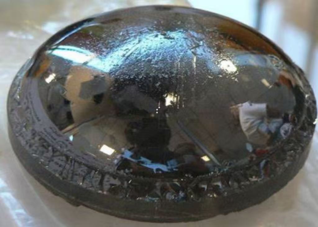
3. Crystal Processing Challenges
Since the hardness of silicon carbide is second only to diamond, which greatly increases the difficulty of cutting. During the slicing process, significant cutting loss occurs, with the loss rate reaching around 40%, resulting in extremely low material utilization efficiency. Due to its low fracture toughness, silicon carbide is prone to cracking and edge chipping during thinning processing. Moreover, subsequent semiconductor manufacturing processes impose extremely stringent requirements on the machining precision and surface quality of silicon carbide substrates, especially regarding surface roughness, flatness, and warpage. This presents considerable pocessing challenges for the thinning, grinding, and polishing of silicon carbide substrates.
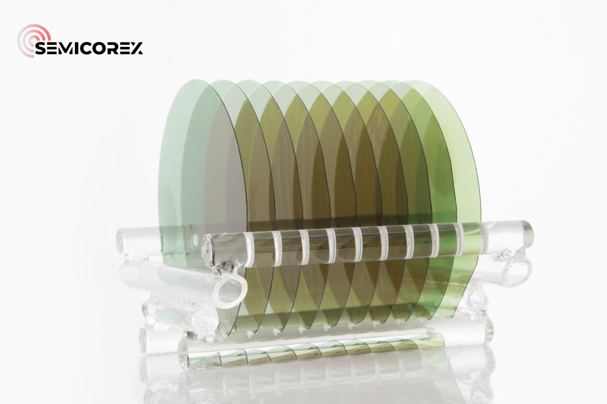
Semicorex offers silicon carbide substrates in various sizes and grades. Please feel free to contact us with any questions or for further details.
Tel: +86-13567891907
Email: sales@semicorex.com
Previous:What are Carbon-Ceramic Brake Discs?


