
- English
- Español
- Português
- русский
- Français
- 日本語
- Deutsch
- tiếng Việt
- Italiano
- Nederlands
- ภาษาไทย
- Polski
- 한국어
- Svenska
- magyar
- Malay
- বাংলা ভাষার
- Dansk
- Suomi
- हिन्दी
- Pilipino
- Türkçe
- Gaeilge
- العربية
- Indonesia
- Norsk
- تمل
- český
- ελληνικά
- український
- Javanese
- فارسی
- தமிழ்
- తెలుగు
- नेपाली
- Burmese
- български
- ລາວ
- Latine
- Қазақша
- Euskal
- Azərbaycan
- Slovenský jazyk
- Македонски
- Lietuvos
- Eesti Keel
- Română
- Slovenski
- मराठी
- Srpski језик

What is wafer bonding technology?
Wafer bonding is a vital important technology in semiconductor manufacturing. It uses physical or chemical methods to bond two smooth and clean wafers together to achieve specific functions or assist in the semiconductor manufacturing process. It is an technology to promote the development of semiconductor technology towards high performance, miniaturization and integration, and is widely used in the manufacture of microelectromechanical systems (MEMS), nanoelectromechanical systems (NEMS), microelectronics and optoelectronics.
Wafer bonding technologies are categorized into temporary bonding and permanent bonding.
Temporary bonding is a process used to reduce risks in ultra-thin wafer processing by bonding it to a carrier surface before thinning to provide mechanical support (but not electrical connection). After mechanical support is completed, a debonding process is required by using thermal, laser and chemical methods.
Permanent bonding is a process used in 3D integration, MEMS, TSV and other device packaging processes to form an irreversible mechanical structure bond. Permanent bonding is divided into the following two categories based on whether there is an intermediate layer:
1. Direct bonding without an intermediate layer
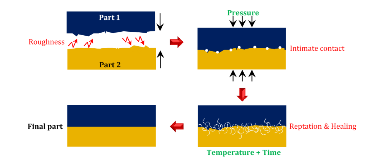
1) Fusion bonding is used in SOI wafer manufacturing, MEMS, Si-Si or SiO₂-SiO₂ bonding.
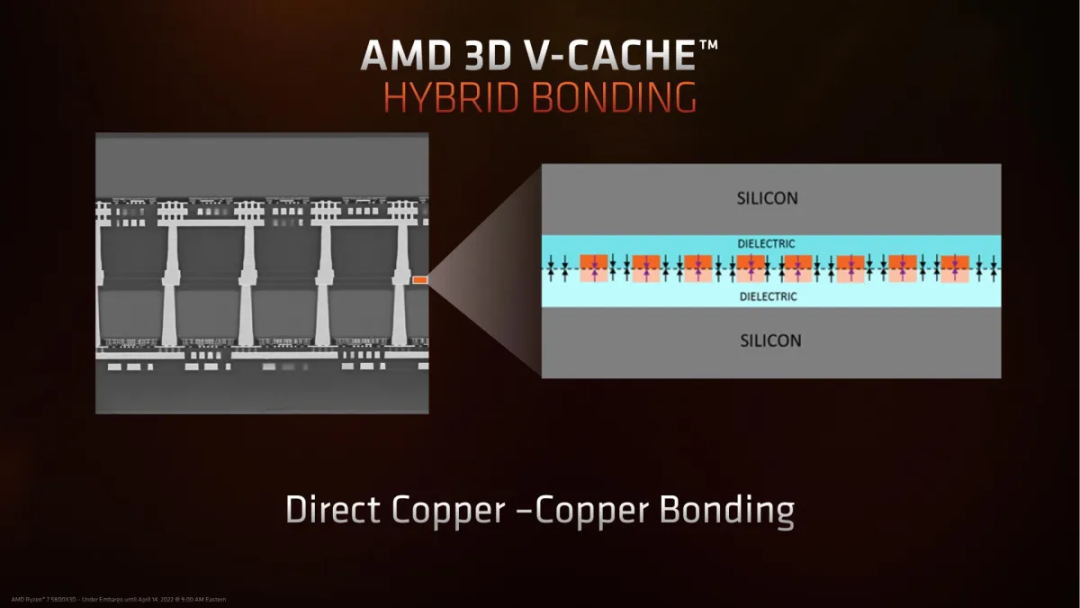
2) Hybrid bonding is used in advanced packaging processes, such as TSV, HBM.
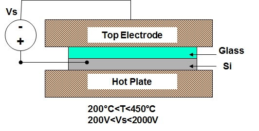
3) Anodic bonding is used in display panels and MEMS.
2. Direct bonding with an intermediate layer
1) Glass paste bonding is used in display panels and MEMS.
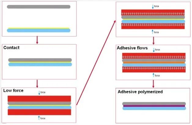
2) Adhesive bonding is used in wafer-level packaging(MLP).
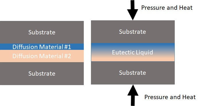
3) Eutectic bonding is used in MEMS packaging and optoelectronic devices.
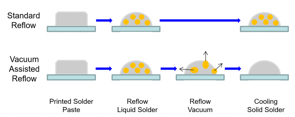
4) Reflow soldering bonding is used in WLP and micro-bump bonding.
5) Metal thermal compression bonding is used in HBM stacking, COWOS, FO-WLP.
Previous:Showerheads in Etching


