
- English
- Español
- Português
- русский
- Français
- 日本語
- Deutsch
- tiếng Việt
- Italiano
- Nederlands
- ภาษาไทย
- Polski
- 한국어
- Svenska
- magyar
- Malay
- বাংলা ভাষার
- Dansk
- Suomi
- हिन्दी
- Pilipino
- Türkçe
- Gaeilge
- العربية
- Indonesia
- Norsk
- تمل
- český
- ελληνικά
- український
- Javanese
- فارسی
- தமிழ்
- తెలుగు
- नेपाली
- Burmese
- български
- ລາວ
- Latine
- Қазақша
- Euskal
- Azərbaycan
- Slovenský jazyk
- Македонски
- Lietuvos
- Eesti Keel
- Română
- Slovenski
- मराठी
- Srpski језик

Core Applications of Alumina Ceramic Components in the Semiconductor
Against the backdrop of continuous expansion of global semiconductor production capacity and relentless advancement of manufacturing processes, semiconductor fabrication equipment now demands unprecedented performance from its core components. During wafer processing, the interior of equipment chambers is exposed to multiple harsh operating conditions, including high-energy plasma bombardment, corrosive gas erosion, extreme temperature fluctuations and stringent cleanliness control. Traditional metallic and organic materials can no longer deliver a combined set of properties such as corrosion resistance, high temperature resistance, superior insulation and low contamination.
As a leading advanced ceramic for semiconductor applications, alumina ceramics strike an optimal balance between cost, machinability and overall performance. Featuring high hardness, excellent insulation, outstanding corrosion resistance and low thermal expansion, they fully meet the stringent requirements for large-size and high-strength components in semiconductor packaging and fabrication equipment, and have become irreplaceable structural materials in the industry.
Core Applications of Alumina Ceramic Components in the Semiconductor
1. Applications in Lithography Equipment
Lithography is one of the most sophisticated processes in semiconductor manufacturing, which imposes extremely strict standards for motion positioning accuracy and cleanliness. Alumina ceramics are widely used for wafer chucks, ceramic stages, precision handling arms and other key parts.
For wafer transportation, alumina ceramics are adopted to fabricate robotic arms. While silicon carbide ceramics are theoretically ideal for such components, alumina ceramic arms deliver superior cost-effectiveness thanks to lower material costs and easier machining. In wafer polishing processes, alumina ceramics are extensively applied to polishing plates, conditioner platforms and vacuum chucks.
The positioning accuracy of lithography stages and wafer transfer systems directly impacts overlay accuracy and production yield. Thanks to its high rigidity, low thermal expansion and excellent vibration resistance, alumina ceramics help the motion systems maintain long-term high-precision operation at high speeds. Meanwhile, the material satisfies strict cleanroom requirements including particle-free performance, non-magnetism and low outgassing.

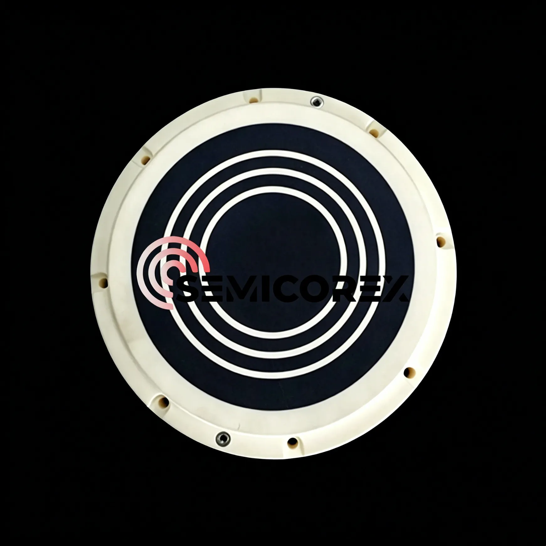
2. Applications in Etching Equipment
Etching is a core semiconductor manufacturing process, where high-energy plasma selectively removes material from designated areas on wafer surfaces. Generated by ionized halogen and inert gases, the plasma not only acts on wafers, but also causes continuous physical and chemical erosion to chamber walls and critical components. This leads to two major issues: eroded parts produce airborne particles that may adhere to wafers and cause chip short circuits; in addition, component wear accelerates equipment aging and shortens service life.
Alumina (Al₂O₃) boasts high dielectric strength and superior chemical resistance, maintaining stable performance under intense plasma exposure. It is one of the most widely used materials for plasma etching protection. High-purity alumina coatings and solid alumina ceramics are commonly used to protect etching chambers and internal components. Beyond chamber structures, alumina ceramics are also adopted for gas nozzles, gas distribution plates and wafer retention rings in plasma processing equipment.
3. Applications in CMP Equipment
In Chemical Mechanical Polishing (CMP), abrasive particles in slurry cause constant friction and wear on polishing plates and stages. Given its exceptional hardness and wear resistance, alumina ceramics are widely used for ceramic polishing tables, polishing plates, lapping plates and end-effectors.
The outstanding surface hardness of alumina polishing tables ensures consistent flatness after processing large batches of wafers, which is critical for precise control of chip surface planarity.

4. Applications in Semiconductor Packaging
In semiconductor packaging, alumina ceramics are widely manufactured into packaging substrates, heat sinks and base plates for high-power electronic devices. Alumina circuit substrates offer excellent insulation, decent thermal conductivity, low thermal expansion coefficient and high mechanical strength, making them a mainstream choice for electronic packaging. Alumina components for bare chip packaging feature excellent airtightness even at elevated temperatures, and are widely used in vacuum electronic environments.
Furthermore, alumina ceramic parts serve as key components in semiconductor back-end equipment, such as ceramic capillaries for wire bonding machines, ceramic nozzles and probe cards for test handlers, all of which require ultra-high precision, great wear resistance and reliable electrical insulation.


