- English
- Español
- Português
- русский
- Français
- 日本語
- Deutsch
- tiếng Việt
- Italiano
- Nederlands
- ภาษาไทย
- Polski
- 한국어
- Svenska
- magyar
- Malay
- বাংলা ভাষার
- Dansk
- Suomi
- हिन्दी
- Pilipino
- Türkçe
- Gaeilge
- العربية
- Indonesia
- Norsk
- تمل
- český
- ελληνικά
- український
- Javanese
- فارسی
- தமிழ்
- తెలుగు
- नेपाली
- Burmese
- български
- ລາວ
- Latine
- Қазақша
- Euskal
- Azərbaycan
- Slovenský jazyk
- Македонски
- Lietuvos
- Eesti Keel
- Română
- Slovenski
- मराठी
- Srpski језик

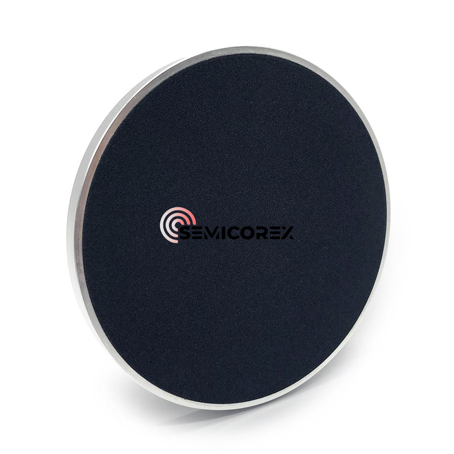
Ceramic Vacuum Chucks
Ceramic vacuum chucks are tools used for clamping and carrying semiconductor wafers in semiconductor wafer manufacturing. They feature high flatness and parallelism, dense and uniform structure, high strength, good air permeability, uniform adsorption force, and ease of trimming. They are suitable for processes such as thinning, cutting, grinding, cleaning, and processing in semiconductor wafer manufacturing, effectively solving many problems such as wafer imprints, chip electrostatic breakdown, and particle contamination. In practical applications, they achieve extremely high processing quality for semiconductor wafers.
Role of ceramic vacuum chuck
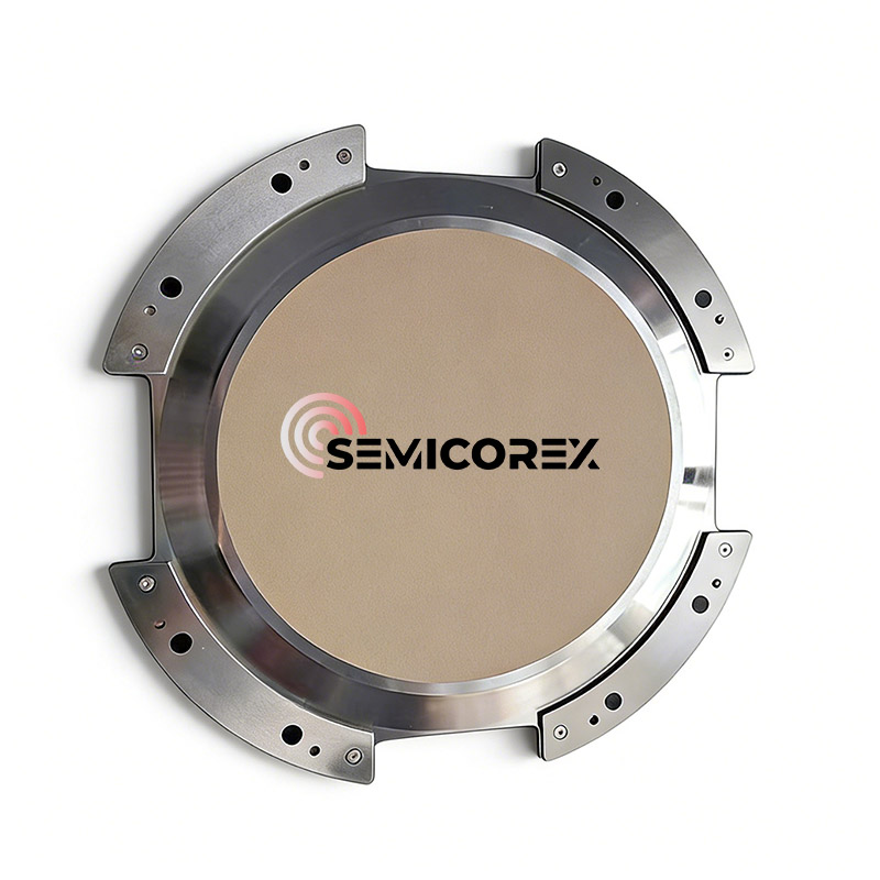
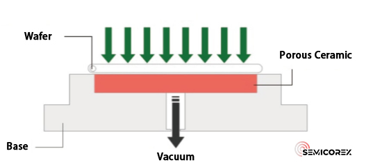
A ceramic vacuum chuck is an ultra-precision process fixture based on the principle of vacuum adsorption. It is primarily made of advanced ceramic materials such as alumina, aluminum nitride, or silicon carbide. Through precisely machined vacuum channels or porous structures on its adsorption surface, it connects to an external vacuum system to form a uniform negative pressure field.
In high-end manufacturing such as semiconductors and display panels, the core value of ceramic vacuum chucks lies in their ability to eliminate traditional mechanical clamping methods. Using only uniformly distributed adsorption force, they can firmly hold ultra-thin and ultra-fragile wafers or glass substrates without contact or particulate contamination throughout the entire process. Simultaneously, thanks to its nanoscale surface flatness, extremely high rigidity, and excellent thermochemical stability, it can provide a near-perfect positioning reference surface for the workpiece in harsh process environments, thereby ensuring the accuracy and yield of critical processes such as photolithography, inspection, and grinding.
Why ceramic
In high-end manufacturing scenarios, chucks are not simply "adsorption tools," but rather crucial fixtures that directly determine process stability and product yield. Among numerous materials, ceramic materials are widely chosen, precisely reflecting how advanced ceramic materials systematically address industry pain points. From an engineering perspective, this can be summarized as "four high" requirements:
(1) High flatness and high rigidity
In semiconductor and display manufacturing processes, the silicon wafers and glass substrates being handled and processed are often extremely thin, with thicknesses as low as tens of micrometers. At such scales, any minute bending, vibration, or uneven local stress can lead to wafer breakage, warping, or even directly affect the alignment accuracy of critical processes such as photolithography.
Advanced ceramic materials (such as alumina and silicon carbide) can achieve sub-micrometer or even nanometer-level flatness through precision sintering and high-precision grinding and polishing processes. Simultaneously, their high elastic modulus endows the chuck with extremely high structural rigidity, ensuring almost no deformation under vacuum adsorption, thus providing an absolutely stable reference plane for the process.
(2) High Cleanliness and Chemical Inertness
Semiconductor manufacturing workshops have extremely stringent cleanliness requirements. Process fixtures must not only be free from particulate contamination but also prevent the release of metal ions and withstand repeated exposure to various cleaning chemicals.
Ceramics, as inorganic non-metallic materials, have a dense and smooth surface, making them less prone to particle generation. Furthermore, they are non-magnetic, contain no migratable metal elements, and exhibit extremely high chemical stability. They maintain stable performance in strong acids, strong alkalis, and organic solvent environments, making them ideal for long-term application in high-level cleanroom processes.
(3) High Durability and Long-Term Stability
On automated production lines operating 24/7, ceramic chucks need to withstand thousands of adsorption and release cycles and face long-term temperature fluctuations and even high-temperature process environments. This places extremely high demands on the material's wear resistance, fatigue resistance, and thermal stability.
Compared to metals or polymers, ceramics have higher hardness and wear resistance, and their thermal expansion behavior is stable, making them less prone to creep or performance degradation. Its lifespan is typically significantly longer than that of traditional material chucks, with lower maintenance and replacement frequency, making it more economical in terms of total lifecycle cost.
(4) Highly Integrated Functional Design
In more advanced semiconductor processes, the function of ceramic chucks is no longer limited to vacuum adsorption. For example, in vacuum chambers used for dry etching and thin film deposition (CVD/PVD), traditional vacuum adsorption holes may disrupt the atmosphere and pressure distribution within the chamber.
At this point, the "electrostatic chuck (ESC)" becomes a key solution. ESCs utilize the electrostatic force generated by the ceramic dielectric layer under an applied electric field to adsorb wafers. This not only avoids the interference of vacuum holes on the process environment but also integrates heaters and cooling channels inside the chuck, enabling precise temperature control of the wafer (from low temperatures to above 500°C), a crucial foundation for the successful implementation of advanced processes.
Application scenario
Ceramic chucks are widely used in high-end manufacturing fields such as semiconductors, display panels, photovoltaics, and precision optics.
In semiconductor processes, they serve as crucial platforms for photolithography, etching, polishing, and inspection. In the display panel industry, they provide stable support and transport for large-size, ultra-thin glass substrates. In photovoltaic cell production, they ensure the safe handling of thin, fragile silicon wafers during cutting and testing.
Their core value lies in providing a precision fixing solution for ultra-thin, ultra-flat, and ultra-brittle workpieces without mechanical stress or particulate contamination, forming the cornerstone of ensuring high yield and efficiency in modern precision manufacturing.