
- English
- Español
- Português
- русский
- Français
- 日本語
- Deutsch
- tiếng Việt
- Italiano
- Nederlands
- ภาษาไทย
- Polski
- 한국어
- Svenska
- magyar
- Malay
- বাংলা ভাষার
- Dansk
- Suomi
- हिन्दी
- Pilipino
- Türkçe
- Gaeilge
- العربية
- Indonesia
- Norsk
- تمل
- český
- ελληνικά
- український
- Javanese
- فارسی
- தமிழ்
- తెలుగు
- नेपाली
- Burmese
- български
- ລາວ
- Latine
- Қазақша
- Euskal
- Azərbaycan
- Slovenský jazyk
- Македонски
- Lietuvos
- Eesti Keel
- Română
- Slovenski
- मराठी
- Srpski језик

Understanding Dry Etching Technology in the Semiconductor Industry
Etching refers to the technique of selectively removing material through physical or chemical means to achieve the designed structural patterns.
Currently, many semiconductor devices employ mesa device structures, which are predominantly created through two types of etching: wet etching and dry etching. While the simple and rapid wet etching plays a significant role in semiconductor device fabrication, it has inherent drawbacks such as isotropic etching and poor uniformity, which result in limited control when transferring small-sized patterns. Dry etching, however, with its high anisotropy, good uniformity, and repeatability, has become prominent in semiconductor device fabrication processes. The term “dry etching” broadly refers to any non-wet etching technology used for removing surface materials and transferring micro and nano patterns, including laser etching, plasma etching, and chemical vapor etching. The dry etching discussed in this text specifically pertains to the narrow application of processes using plasma discharge—either physical or chemical—to modify material surfaces. It covers several common industrial etching technologies, including Ion Beam Etching (IBE), Reactive Ion Etching (RIE), Electron Cyclotron Resonance (ECR) plasma etching, and Inductively Coupled Plasma (ICP) etching.
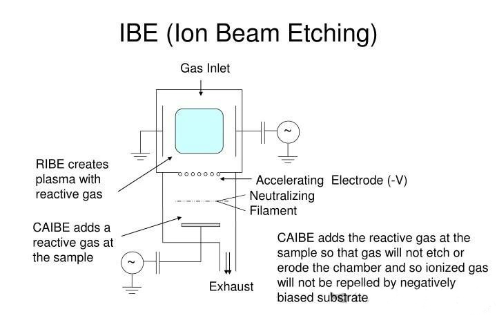
1. Ion Beam Etching (IBE)
Also known as ion milling, IBE developed in the 1970s as a purely physical etching method. The process involves ion beams created from inert gases (like Ar, Xe) that are accelerated by a voltage to bombard the target material’s surface. The ions transfer energy to the surface atoms, causing those with energy exceeding their binding energy to sputter away. This technique employs accelerated voltage to control the direction and energy of the ion beam, resulting in excellent etch anisotropy and rate controllability. While it is ideal for etching chemically stable materials such as ceramics and certain metals, the need for thicker masks for deeper etches may compromise etching precision, and the high-energy ion bombardment may cause unavoidable electrical damage due to lattice disruptions.
2. Reactive Ion Etching (RIE)
Developed from IBE, RIE combines chemical reactions with physical ion bombardment. Compared to IBE, RIE offers higher etching rates and excellent anisotropy and uniformity across large areas, making it one of the most extensively used etching techniques in micro and nano fabrication. The process involves applying radio frequency (RF) voltage to parallel plate electrodes, causing electrons in the chamber to accelerate and ionize the reaction gases, leading to a stable plasma state on one side of the plates. The plasma carries a positive potential due to electrons being attracted to the cathode and grounded at the anode, thus creating an electric field across the chamber. The positively charged plasma accelerates towards the cathode-linked substrate, effectively etching it.
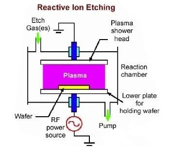
During the etching process, the chamber maintains a low-pressure environment (0.1~10 Pa), which enhances the ionization rate of the reaction gases and accelerates the chemical reaction process at the substrate surface. Generally, the RIE process requires the reaction by-products to be volatile to be efficiently removed by the vacuum system, ensuring high etching precision. The RF power level directly determines the plasma density and the acceleration bias voltage, thereby controlling the etching rate. However, while increasing plasma density, RIE also increases the bias voltage, which can cause lattice damage and reduce the selectivity of the mask, thus posing limitations for etching applications. With the rapid development of large-scale integrated circuits and the decreasing size of transistors, there has been a greater demand for precision and aspect ratios in micro and nano fabrication, leading to the advent of high-density plasma-based dry etching technologies, providing new opportunities for the advancement of electronic information technology.
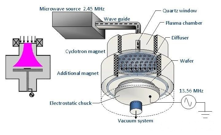
3. Electron Cyclotron Resonance (ECR) Plasma Etching
ECR technology, an early method for achieving high-density plasma, utilizes microwave energy to resonate with electrons within the chamber, enhanced by an externally applied, frequency-matched magnetic field to induce electron cyclotron resonance. This method achieves significantly higher plasma densities than RIE, enhancing the etching rate and mask selectivity, thus facilitating the etching of ultra-high aspect ratio structures. However, the complexity of the system, which relies on coordinated function of microwave sources, RF sources, and magnetic fields, poses operational challenges. The emergence of Inductively Coupled Plasma (ICP) etching soon followed as a simplification over ECR.
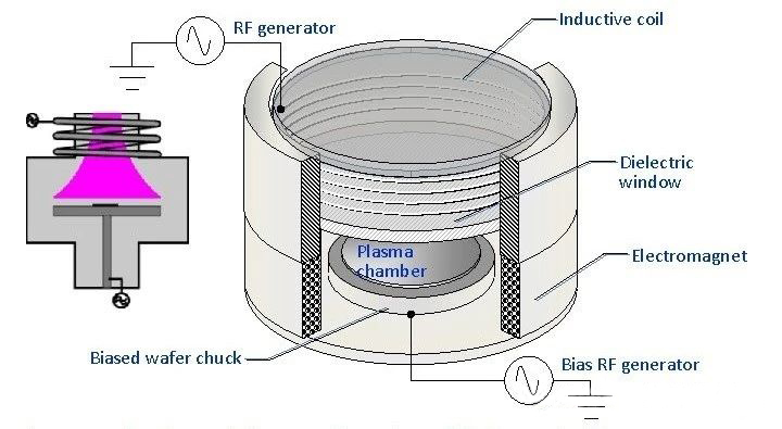
4. Inductively Coupled Plasma (ICP) Etching
ICP etching technology simplifies the system based on ECR technology by using two 13.56MHz RF sources to control both plasma generation and the acceleration bias voltage. Instead of the external magnetic field used in ECR, a spiral coil induces an alternating electromagnetic field, as shown in the schematic. The RF sources transfer energy through electromagnetic coupling to the internal electrons, which move in a cyclotron motion within the induced field, colliding with the reaction gases to cause ionization. This setup achieves plasma densities comparable to ECR. ICP etching combines the advantages of various etching systems, meeting the needs for high etch rates, high selectivity, large-area uniformity, and simple, controllable equipment structure, thus rapidly becoming the preferred choice for a new generation of high-density plasma etching technologies.
5. Characteristics of Dry Etching
Dry etching technology has rapidly taken a principal position in micro and nanofabrication due to its superior anisotropy and high etching rates, replacing wet etching. The criteria for evaluating good dry etching technology include mask selectivity, anisotropy, etching rate, overall uniformity, and surface smoothness from lattice damage. With many evaluation criteria, the specific situation must be considered based on fabrication needs. The most direct indicators of dry etching are the surface morphology, including the flatness of the etched floor and sidewalls and the anisotropy of the etched terraces, which can both be controlled by adjusting the ratio of chemical reactions to physical bombardment. Microscopic characterization after etching is typically performed using scanning electron microscopy and atomic force microscopy. Mask selectivity, which is the ratio of the depth of etching of the mask to that of the material under the same etching conditions and time, is crucial. Generally, the higher the selectivity, the better the accuracy of pattern transfer. Common masks used in ICP etching include photoresist, metals, and dielectric films. Photoresist has poor selectivity and can degrade under high temperatures or energetic bombardment; metals offer high selectivity but pose challenges in mask removal and often require multi-layer masking techniques. Additionally, metal masks may adhere to the sidewalls during etching, forming leakage pathways. Therefore, choosing the appropriate mask technology is especially important for etching, and the selection of mask materials should be determined based on the specific performance requirements of the devices.**


