
- English
- Español
- Português
- русский
- Français
- 日本語
- Deutsch
- tiếng Việt
- Italiano
- Nederlands
- ภาษาไทย
- Polski
- 한국어
- Svenska
- magyar
- Malay
- বাংলা ভাষার
- Dansk
- Suomi
- हिन्दी
- Pilipino
- Türkçe
- Gaeilge
- العربية
- Indonesia
- Norsk
- تمل
- český
- ελληνικά
- український
- Javanese
- فارسی
- தமிழ்
- తెలుగు
- नेपाली
- Burmese
- български
- ລາວ
- Latine
- Қазақша
- Euskal
- Azərbaycan
- Slovenský jazyk
- Македонски
- Lietuvos
- Eesti Keel
- Română
- Slovenski
- मराठी
- Srpski језик

Porous Graphite for High Quality SiC Crystal Growth by PVT Method
Silicon Carbide (SiC) has emerged as a key material in the field of semiconductor technology, offering exceptional properties that make it highly desirable for various electronic and optoelectronic applications. The production of high-quality SiC single crystals is crucial for advancing the capabilities of devices such as power electronics, LEDs, and high-frequency devices. In this article, we delve into the significance of porous graphite in the Physical Vapor Transport (PVT) method for 4H-SiC single crystal growth.
The PVT method is a widely employed technique for the production of SiC single crystals. This process involves the sublimation of SiC source materials in a high-temperature environment, followed by their condensation on a seed crystal to form a single crystal structure. The success of this method relies heavily on the conditions within the growth chamber, including temperature, pressure, and the materials used.
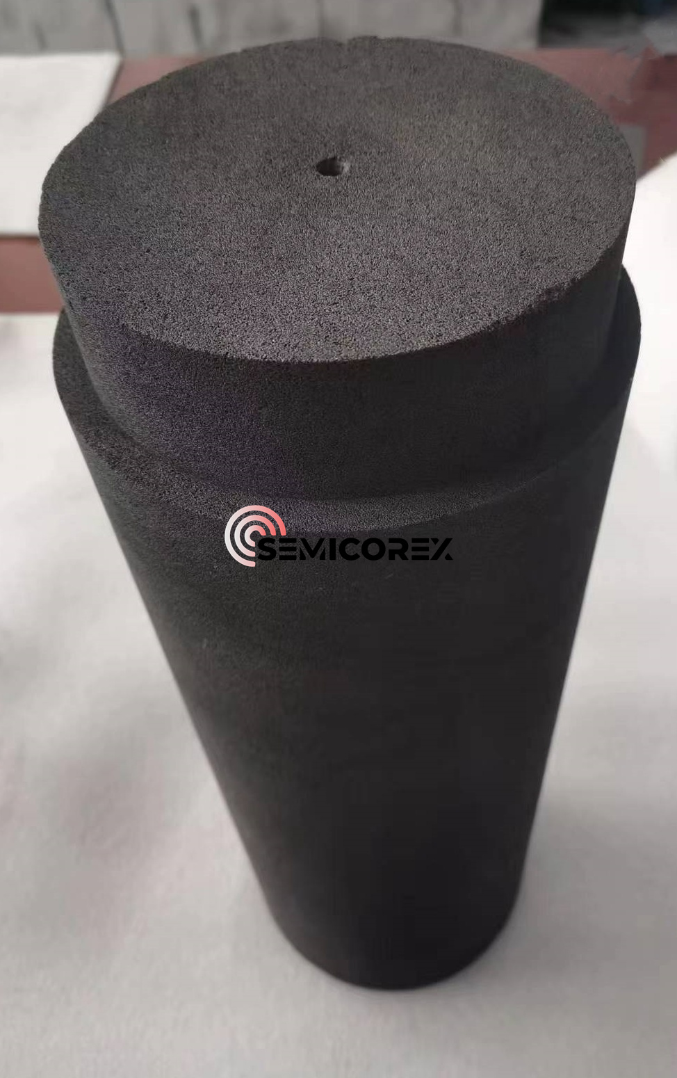
Porous graphite, with its unique structure and properties, plays a pivotal role in enhancing the SiC crystal growth process. SiC crystals grown by traditional PVT methods will have multiple crystal forms. However, using porous graphite crucible in the furnace can greatly increace the purity of 4H-SiC single crystal.
The incorporation of porous graphite in the PVT method for 4H-SiC single crystal growth represents a significant advancement in the field of semiconductor technology. The unique properties of porous graphite contribute to enhanced gas flow, temperature homogeneity, stress reduction, and improved heat dissipation. These factors collectively result in the production of high-quality SiC single crystals with fewer defects, paving the way for the development of more efficient and reliable electronic and optoelectronic devices. As the semiconductor industry continues to evolve, the utilization of porous graphite in SiC crystal growth processes is poised to play a pivotal role in shaping the future of electronic materials and devices.
Previous:What is isostatic graphite?


