
- English
- Español
- Português
- русский
- Français
- 日本語
- Deutsch
- tiếng Việt
- Italiano
- Nederlands
- ภาษาไทย
- Polski
- 한국어
- Svenska
- magyar
- Malay
- বাংলা ভাষার
- Dansk
- Suomi
- हिन्दी
- Pilipino
- Türkçe
- Gaeilge
- العربية
- Indonesia
- Norsk
- تمل
- český
- ελληνικά
- український
- Javanese
- فارسی
- தமிழ்
- తెలుగు
- नेपाली
- Burmese
- български
- ລາວ
- Latine
- Қазақша
- Euskal
- Azərbaycan
- Slovenský jazyk
- Македонски
- Lietuvos
- Eesti Keel
- Română
- Slovenski
- मराठी
- Srpski језик

Introducing Physical Vapor Transport (PVT)
SiC's own characteristics determine its single crystal growth is more difficult. Due to the absence of Si:C=1:1 liquid phase at atmospheric pressure, the more mature growth process adopted by the mainstream of the semiconductor industry can not be used to grow the more mature growth method-straight pulling method, the descending crucible method and other methods for growth. After theoretical calculations, only when the pressure is greater than 105 atm and the temperature is higher than 3200 ℃, can we get the stoichiometric ratio of Si:C = 1:1 solution. pvt method is currently one of the more mainstream methods.
The PVT method has low requirements for growth equipment, simple and controllable process, and the technology development is relatively mature, and has already been industrialized.The structure of the PVT method is shown in the figure below.
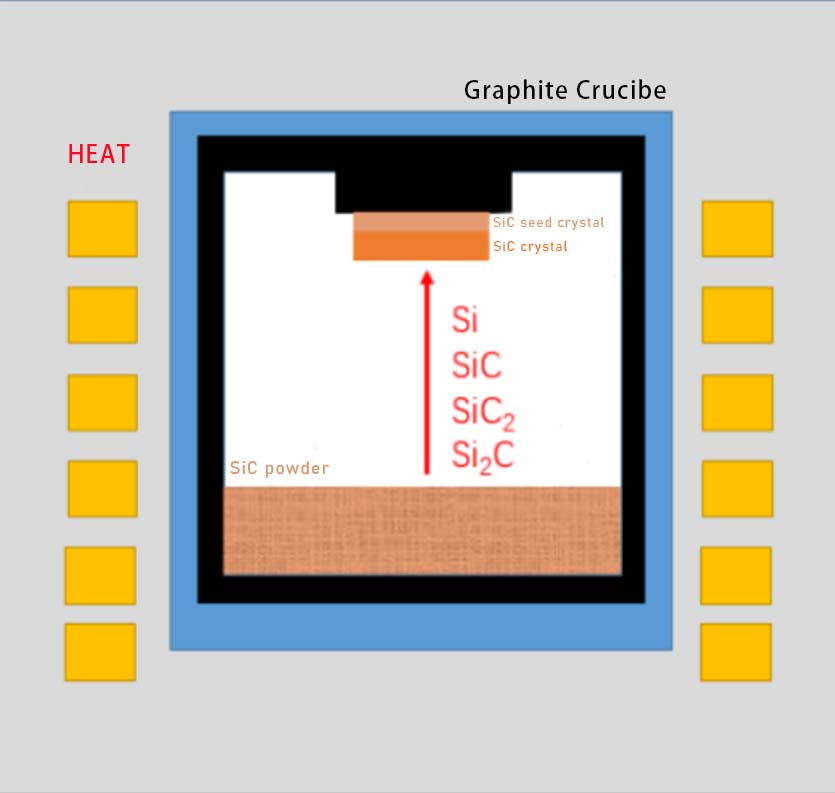
The regulation of axial and radial temperature field can be realized by controlling the external heat preservation condition of graphite crucible. The SiC powder is placed at the bottom of the graphite crucible with higher temperature, and the SiC seed crystal is fixed at the top of the graphite crucible with lower temperature. The distance between the powder and the seed crystals is generally controlled to be tens of millimeters to avoid contact between the growing single crystal and the powder.
The temperature gradient is usually in the range of 15-35°C/cm interval. Inert gas at a pressure of 50-5000 Pa is retained in the furnace to increase convection. The SiC powder is heated to 2000-2500°C by different heating methods (induction heating and resistance heating, the corresponding equipment is induction furnace and resistance furnace), and the raw powder sublimates and decomposes into gas-phase components such as Si, Si2C, SiC2, etc., which are transported to the seed crystal end with gas convection, and SiC crystals are crystallized on the seed crystals to achieve single crystal growth. Its typical growth rate is 0.1-2mm/h.
At present, the PVT method has been developed and matured, and can realize the mass production of hundreds of thousands of pieces per year, and its processing size has been realized 6 inches, and is now developing to 8 inches, and there are also related companies using the realization of the 8-inch substrate chip samples. However, PVT method still has the following problems:
- Large size SiC substrate preparation technology is still immature. Because the PVT method can only be in the longitudinal long thick, it is difficult to realize the transverse expansion. To obtain a larger diameter SiC wafers often need to invest huge amounts of money and effort, and with the current SiC wafer size continues to expand, this difficulty will only gradually increase. (Same as the development of Si).
- The current level of defects on SiC substrates grown by the PVT method is still high. Dislocations reduce the blocking voltage and increase the leakage current of SiC devices, which affects the application of SiC devices.
- P-type substrates are difficult to prepare by PVT. Currently SiC devices are mainly unipolar devices. Future high-voltage bipolar devices will require p-type substrates. The use of p-type substrate can realize the growth of N-type epitaxial, compared with the growth of P-type epitaxial on N-type substrate has a higher carrier mobility, which can further improve the performance of SiC devices.


