
- English
- Español
- Português
- русский
- Français
- 日本語
- Deutsch
- tiếng Việt
- Italiano
- Nederlands
- ภาษาไทย
- Polski
- 한국어
- Svenska
- magyar
- Malay
- বাংলা ভাষার
- Dansk
- Suomi
- हिन्दी
- Pilipino
- Türkçe
- Gaeilge
- العربية
- Indonesia
- Norsk
- تمل
- český
- ελληνικά
- український
- Javanese
- فارسی
- தமிழ்
- తెలుగు
- नेपाली
- Burmese
- български
- ລາວ
- Latine
- Қазақша
- Euskal
- Azərbaycan
- Slovenský jazyk
- Македонски
- Lietuvos
- Eesti Keel
- Română
- Slovenski
- मराठी
- Srpski језик

New Research Findings On Graphene
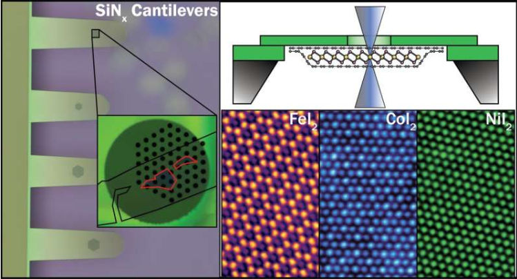
Two-dimensional materials promise revolutionary advancements in electronics and photonics, but many of the most promising candidates degrade within seconds of exposure to air, making them virtually unsuitable for research or integration into practical technologies. Transition metal dihalides are a highly attractive yet challenging class of materials; their predicted properties are well-suited for next-generation devices, but their extremely high reactivity in air even hinders characterization of their fundamental structure.
Researchers at the National Graphene Institute at the University of Manchester have now achieved, for the first time, atomic-resolution imaging of monolayer transition metal diiodides by creating graphene-sealed TEM samples that prevent these highly reactive materials from degrading upon contact with air.
This research, published in ACS Nano, demonstrates that completely encapsulating crystals within graphene maintains atomically clean interfaces and extends their lifespan from seconds to months.
This capability stems from an improvement on the inorganic stamp transfer method previously developed and reported by the team in *Nature Electronics*, which lays the foundation for producing stable, sealed samples.
“Initially, handling these materials was nearly impossible because they would be completely destroyed within seconds of exposure to air, making traditional preparation methods simply unusable,” explained Dr. Wendong Wang, who was involved in developing the transfer technology and preparing the relevant samples. “Our method protects the samples without any unnecessary transfer steps. It enables the preparation of samples that can be preserved not only for hours but also for months, and can be internationally transferred between different institutions, solving a major bottleneck in the field of two-dimensional materials research.”
“Once we were able to prepare stable samples, we were able to make some interesting observations about these materials, including identifying extensive local structural variations, atomic defect dynamics, and edge structure evolution in the thinnest samples,” said Dr. Gareth Teton, who led the transmission electron microscopy imaging and analysis for this work.
Picture by University of Manchester
“The structure of two-dimensional materials is closely related to their properties. Therefore, being able to directly observe the structures of different crystals (from monolayers to bulk thicknesses) and their defect behavior is expected to provide information for further research on these materials, thereby unlocking their potential in the technological field.”
“What excites me most is that this research opens up previously inaccessible scientific areas. We theoretically know that many active two-dimensional materials have outstanding performance in electronics, optoelectronics, and quantum applications, but we have been unable to obtain stable samples in the laboratory to verify these predictions,” commented Professor Roman Gorbachev of the National Graphene Institute, who led the research.
Previous:What are the LPCVD Processes?


