
- English
- Español
- Português
- русский
- Français
- 日本語
- Deutsch
- tiếng Việt
- Italiano
- Nederlands
- ภาษาไทย
- Polski
- 한국어
- Svenska
- magyar
- Malay
- বাংলা ভাষার
- Dansk
- Suomi
- हिन्दी
- Pilipino
- Türkçe
- Gaeilge
- العربية
- Indonesia
- Norsk
- تمل
- český
- ελληνικά
- український
- Javanese
- فارسی
- தமிழ்
- తెలుగు
- नेपाली
- Burmese
- български
- ລາວ
- Latine
- Қазақша
- Euskal
- Azərbaycan
- Slovenský jazyk
- Македонски
- Lietuvos
- Eesti Keel
- Română
- Slovenski
- मराठी
- Srpski језик

What is CVD process in semiconductor?
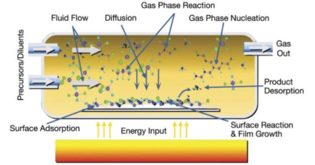
Chemical vapor deposition CVD refers to the introduction of two or more gaseous raw materials into a reaction chamber under vacuum and high temperature conditions, where the gaseous raw materials react with each other to form a new material, which is deposited on the wafer surface. Characterized by a wide range of applications, no need for high vacuum, simple equipment, good controllability and repeatability, and suitability for mass production. Mainly used for the growth of thin films of dielectric/insulating materials, including Low Pressure CVD (LPCVD), Atmospheric Pressure CVD (APCVD), Plasma Enhanced CVD (PECVD), Metal Organic CVD (MOCVD), Laser CVD (LCVD) and etc.
Atomic Layer Deposition (ALD) is a method of plating substances onto a substrate surface layer by layer in the form of a single atomic film. It is an atomic scale thin film preparation technique, which is essentially a type of CVD, and is characterized by the deposition of ultra-thin thin films of uniform, controllable thickness and adjustable composition. With the development of nanotechnology and semiconductor microelectronics, the size requirements of devices and materials continue to decrease, while the width-to-depth ratio of device structures continues to increase, which requires the thickness of the materials used to be reduced to the teens of nanometers to a few nanometers order of magnitude. Compared with the traditional deposition process, ALD technology has excellent step coverage, uniformity and consistency, and can deposit structures with width-to-depth ratios of up to 2000:1, so it has gradually become an irreplaceable technology in the related manufacturing fields, with great potential for development and application space.
Metal Organic Chemical Vapor Deposition (MOCVD) is the most advanced technology in the field of chemical vapor deposition. Metal Organic Chemical Vapor Deposition (MOCVD) is the process of depositing elements of group III and II and elements of group V and VI on the substrate surface by thermal decomposition reaction, taking elements of group III and II and elements of group V and VI as the growth source materials. MOCVD involves the deposition of Group III and II elements and Group V and VI elements as growth source materials on the substrate surface through thermal decomposition reaction to grow various thin layers of Group III-V (GaN, GaAs, etc.), Group II-VI (Si, SiC, etc.), and multiple solid solutions. and multivariate solid solution thin single crystal materials, is the main means to produce photoelectric devices, microwave devices, power device materials. It is the main means to produce materials for optoelectronic devices, microwave devices and power devices.
Semicorex is specialized in MOCVD SiC coatings for semiconductor process. If you have any questions or require further information, please feel free to contact us.
Contact phone # +86-13567891907
Email: sales@semicorex.com


