
- English
- Español
- Português
- русский
- Français
- 日本語
- Deutsch
- tiếng Việt
- Italiano
- Nederlands
- ภาษาไทย
- Polski
- 한국어
- Svenska
- magyar
- Malay
- বাংলা ভাষার
- Dansk
- Suomi
- हिन्दी
- Pilipino
- Türkçe
- Gaeilge
- العربية
- Indonesia
- Norsk
- تمل
- český
- ελληνικά
- український
- Javanese
- فارسی
- தமிழ்
- తెలుగు
- नेपाली
- Burmese
- български
- ລາວ
- Latine
- Қазақша
- Euskal
- Azərbaycan
- Slovenský jazyk
- Македонски
- Lietuvos
- Eesti Keel
- Română
- Slovenski
- मराठी
- Srpski језик

What is SOI?
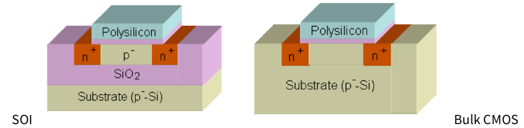
SOI, short for Silicon-On-Insulator, is a semiconductor manufacturing process based on special substrate materials. Since its industrialization in the 1980s, this technology has become an important branch of advanced semiconductor manufacturing processes. Distinguished by its unique three-layer composite structure, SOI process is a significant departure from traditional bulk silicon process.
Composed of a single-crystal silicon device layer, a silicon dioxide insulating layer (also known as a buried oxide layer, BOX), and a silicon substrate, the SOI wafer creates an independent and stable electrical environment. Each layer fulfills a distinct yet complementary role in ensuring the wafer’s performance and reliability:
1.The top single-crystal silicon device layer, which usually has a thickness of 5 nm to 2 μm, serves as the central area for creating active devices like transistors. Its ultra-thinness is the foundation for improved performance and device miniaturization.
2.The primary function of the middle buried oxide layer is to achieve electrical isolation. The BOX layer effectively blocks electrical connections between the device layer and the substrate below by utilizing both physical and chemical isolation mechanisms, with its thickness typically ranging from 5nm to 2μm.
3.Regarding the bottom silicon substrate, its primary function is to offer structural robustness and steady mechanical support, which are crucial assurances for the wafer's dependability during production and later uses. In terms of thickness, it generally falls within the range of 200μm to 700μm.
Advantages of SOI Wafer
1.Low power consumption
The presence of the insulating layer in SOI wafers reduces leakage current and capacitance, contributing to lower device static and dynamic power consumption.
2.Radiation resistance
The insulating layer in SOI wafers can effectively shield cosmic rays and electromagnetic interference, avoiding the impact of extreme environments on device stability, enabling it to operate stably in special fields such as aerospace and nuclear industry.
3.Excellent high-frequency performance
The insulating layer design significantly reduces unwanted parasitic effects caused by the interaction between the device and the substrate. The reduction in parasitic capacitance lowers the latency of SOI devices in high-frequency signal processing (such as 5G communication), thereby improving operating efficiency.
4.Design flexibility
The SOI substrate features inherent dielectric isolation, eliminating the need for doped trench isolation, which simplifies the manufacturing process and improves production yield.
Application of SOI technology
1.Consumer electronics sector: RF front-end modules for smartphones(such as 5G filters).
2.Automotive electronics field: Automotive-grade radar chip.
3.Aerospace: Satellite communication equipment.
4.Medical device field: implantable medical sensors, low-power monitoring chips.


