
- English
- Español
- Português
- русский
- Français
- 日本語
- Deutsch
- tiếng Việt
- Italiano
- Nederlands
- ภาษาไทย
- Polski
- 한국어
- Svenska
- magyar
- Malay
- বাংলা ভাষার
- Dansk
- Suomi
- हिन्दी
- Pilipino
- Türkçe
- Gaeilge
- العربية
- Indonesia
- Norsk
- تمل
- český
- ελληνικά
- український
- Javanese
- فارسی
- தமிழ்
- తెలుగు
- नेपाली
- Burmese
- български
- ລາວ
- Latine
- Қазақша
- Euskal
- Azərbaycan
- Slovenský jazyk
- Македонски
- Lietuvos
- Eesti Keel
- Română
- Slovenski
- मराठी
- Srpski језик

What is Doping Process?
In the manufacture of ultra-high purity wafers, wafers must reach a purity standard of over 99.999999999% to ensure the fundamental properties of semiconductors. Paradoxically, to achieve the functional construction of integrated circuits, specific impurities must be introduced locally onto the surface of wafers through doping processes. This is because pure single-crystal silicon has an extremely low concentration of free carriers at ambient temperature. Its conductivity is close to that of an insulator, making it impossible to form an effective current. The doping process solves this by adjusting the doping elements and doping concentration.
Semicorex offers high-quality SiC solutions for semiconductor diffusion process. If you have any inquiries, please feel free to get in touch with us.
The two mainstream doping techniques:
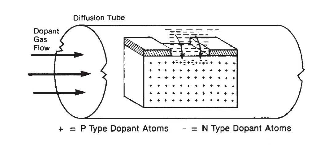
1.High-temperature diffusion is a conventiona method for semiconductor doping. The idea is to treat the semiconductor at a high temperature, which causes impurity atoms to diffuse from the semiconductor's surface into its interior. Since impurity atoms are typically larger than semiconductor atoms, the thermal motion of atoms in the crystal lattice is required to help these impurities occupy interstitial voids. By carefully controlling the temperature and time parameters during the diffusion process, it is possible to effectively control the impurity distribution based on this characteristic.This method can be used to create deep doped junctions, such as the double-well structure in CMOS technology.
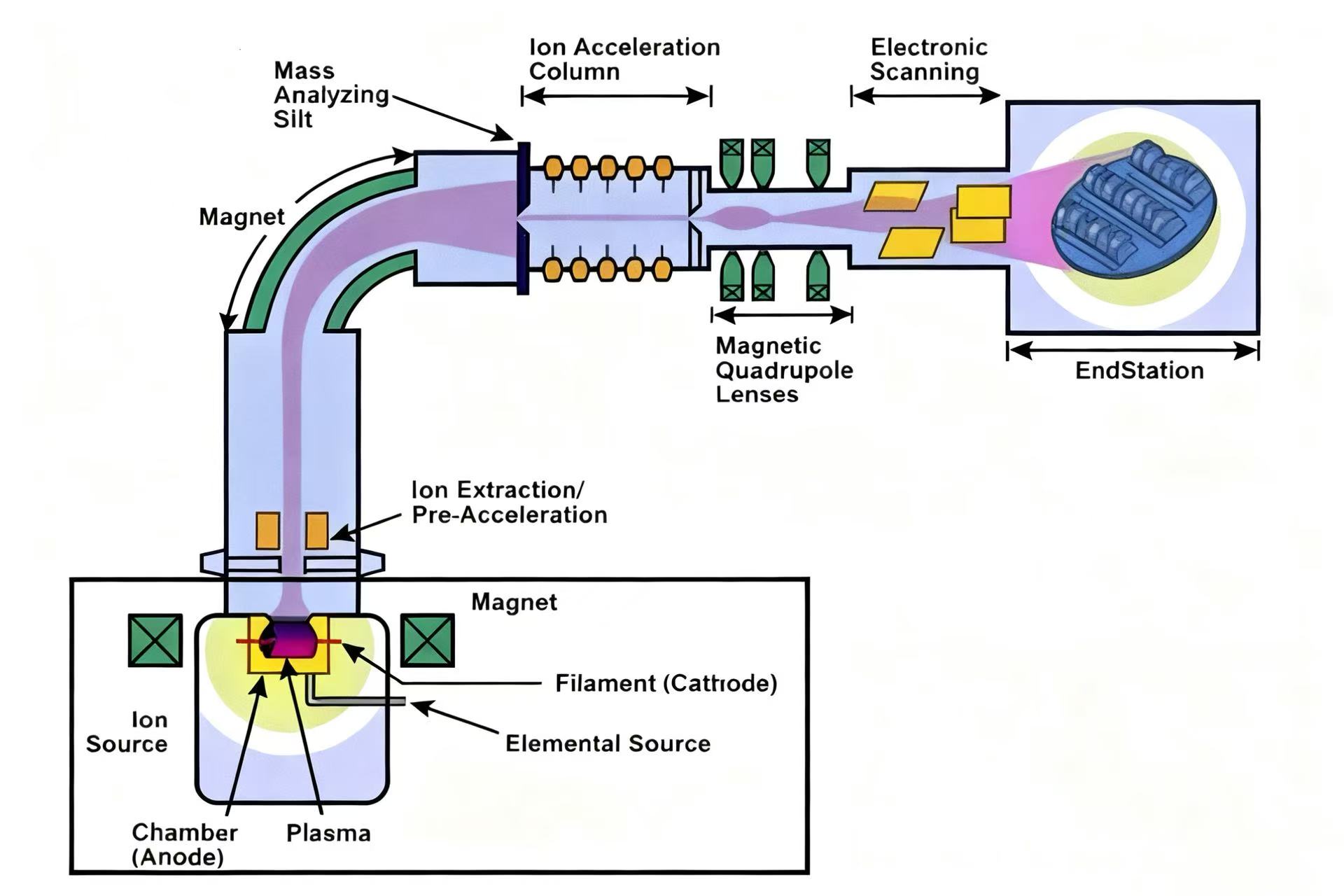
2.Ion implantation is the primary doping technique in semiconductor manufacturing, which has several advantages, such as high doping accuracy, low process temperatures, and little damage to the substrate material. Specifically, the ion implantation process entails ionizing impurity atoms to create charged ions, then accelerating these ions via a high-intensity electric field to form a high-energy ion beam. The semiconductor surface is then struck by these fast-moving ions, allowing for precise implantation with adjustable doping depth. This technique is particularly useful for creating shallow junction structures, such as the source and drain regions of MOSFETs, and allows for high-precision control over the distribution and concentration of impurities.
Doping-related factors:
1. Doping Elements
N-type semiconductors are formed by introducing Group V elements (such as phosphorus and arsenic), while P-type semiconductors are formed by introducing Group III elements (such as boron). Meanwhile, the purity of doping elements directly impacts the quality of the doped material, with high-purity dopants helping reduce extra defects.
2. Doping Concentration
While the low concentration is unable to significantly increase conductivity, the high concentration tends to harm the lattice and raise the risk of leakage.
3. Process Control Parameters
The diffusion effect of impurity atoms is influenced by temperature, time, and atmospheric conditions. In ion implantation, the doping depth and uniformity are determined by ion energy, dose, and incident angle.
Semicorex offers high-quality SiC solutions for semiconductor diffusion process. If you have any inquiries, please feel free to get in touch with us.
Previous:Ceramic Vacuum Chuck


