
- English
- Español
- Português
- русский
- Français
- 日本語
- Deutsch
- tiếng Việt
- Italiano
- Nederlands
- ภาษาไทย
- Polski
- 한국어
- Svenska
- magyar
- Malay
- বাংলা ভাষার
- Dansk
- Suomi
- हिन्दी
- Pilipino
- Türkçe
- Gaeilge
- العربية
- Indonesia
- Norsk
- تمل
- český
- ελληνικά
- український
- Javanese
- فارسی
- தமிழ்
- తెలుగు
- नेपाली
- Burmese
- български
- ລາວ
- Latine
- Қазақша
- Euskal
- Azərbaycan
- Slovenský jazyk
- Македонски
- Lietuvos
- Eesti Keel
- Română
- Slovenski
- मराठी
- Srpski језик

What indicators Should Be Paid Attention To When Selecting Suitable Wafers?
Wafer selection has a significant impact on the development and manufacturing of semiconductor devices. Wafer selection should be guided by the requirements of specific application scenarios, and should be carefully evaluated using the following crucial metrics.
1.Total Thickness Variation:
The difference between the maximum and minimum thicknesses measured across the wafer surface is known as TTV. It is an important metric for measuring thickness uniformity, and higher performance is indicated by smaller values.
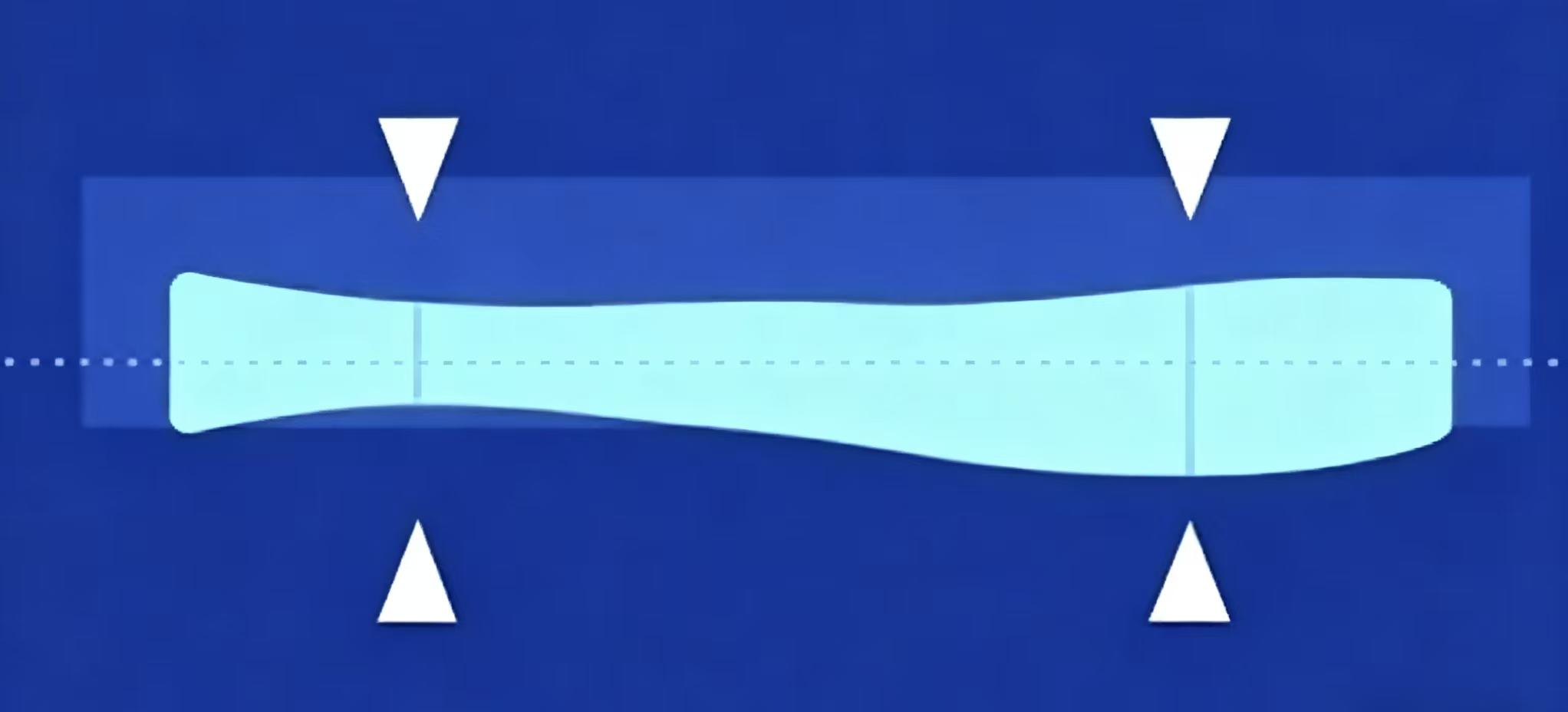
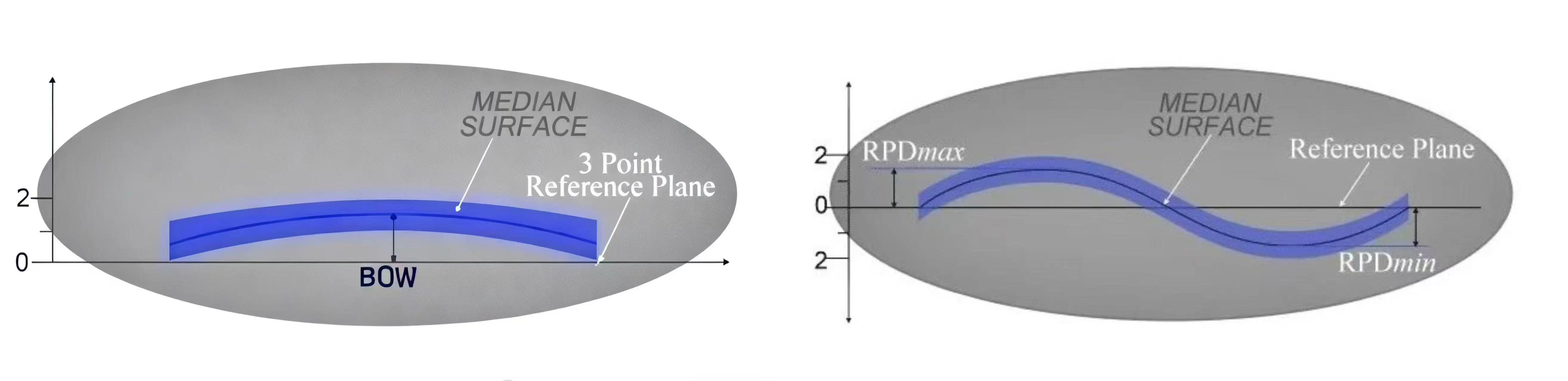
2.Bow and warp:
The bow indicator focuses on the vertical offset of the wafer center area, which only reflects the local bending state. It is suitable for evaluating scenarios that are sensitive to local flatness. The warp indicator is useful for assessing overall flatness and distortion because it considers the deviation of the entire wafer surface and provides information on overall flatness for the entire wafer.
3.Particle:
Particle contamination on the wafer surface can affect device manufacturing and performance, so it is necessary to minimize particle generation during the production process and use special cleaning processes to reduce and remove surface particle contamination.
4.Roughness:
Roughness refers to an indicator that measures the flatness of a wafer surface at the microscopic scale, which is different from the macroscopic flatness. The lower the surface roughness, the smoother the surface. Issues like uneven thin film deposition, blurred photolithographic pattern edges, and poor electrical performance can result from excessive roughness.
5.defects:
Wafer defects refer to incomplete or irregular lattice structures caused by mechanical processing, which in turn form crystal damage layers containing micropipes, dislocations, scratches. It will damage the mechanical and electrical properties of the wafer, and eventually may lead to chip failure.
6.Conductivity Type/dopant:
The two types of wafers are n-type and p-type, depending on the doping components. n-type wafers are typically doped with Group V elements to achieve conductivity. Phosphorus (P), arsenic (As), and antimony (Sb) are common doping elements. P-type wafers are primarily doped with Group III elements, typically boron (B). Undoped silicon is called intrinsic silicon. Its internal atoms are bonded together by covalent bonds to form a solid structure, making it an electrically stable insulator. However, there are no intrinsic silicon wafers that are completely free of impurities in real production.
7.Resistivity:
Controlling the wafer resistivity is essential because it directly affects the performance of semiconductor devices. In order to modify the resistivity of wafers, manufacturers usually dope them. The higher dopant concentrations result in lower resistivity, while lower dopant concentrations result in higher resistivity.
In conclusion, it is recommended that you clarify the subsequent process conditions and equipment limitations before selecting wafers, and then make your selection based on the above indicators to ensure the dual goals of shortening the semiconductor device development cycle and optimizing manufacturing costs.
Previous:Silicon Components for Dry Etching


