
- English
- Español
- Português
- русский
- Français
- 日本語
- Deutsch
- tiếng Việt
- Italiano
- Nederlands
- ภาษาไทย
- Polski
- 한국어
- Svenska
- magyar
- Malay
- বাংলা ভাষার
- Dansk
- Suomi
- हिन्दी
- Pilipino
- Türkçe
- Gaeilge
- العربية
- Indonesia
- Norsk
- تمل
- český
- ελληνικά
- український
- Javanese
- فارسی
- தமிழ்
- తెలుగు
- नेपाली
- Burmese
- български
- ລາວ
- Latine
- Қазақша
- Euskal
- Azərbaycan
- Slovenský jazyk
- Македонски
- Lietuvos
- Eesti Keel
- Română
- Slovenski
- मराठी
- Srpski језик

SiC Ingot Processing
As a representative of third-generation semiconductor materials, silicon carbide (SiC) boasts a wide bandgap, high thermal conductivity, high breakdown electric field, and high electron mobility, making it an ideal material for high-voltage, high-frequency, and high-power devices. It effectively overcomes the physical limitations of traditional silicon-based power semiconductor devices and is hailed as a green energy material driving the "new energy revolution." In the manufacturing process of power devices, the growth and processing of SiC single crystal substrates are critical to performance and yield.
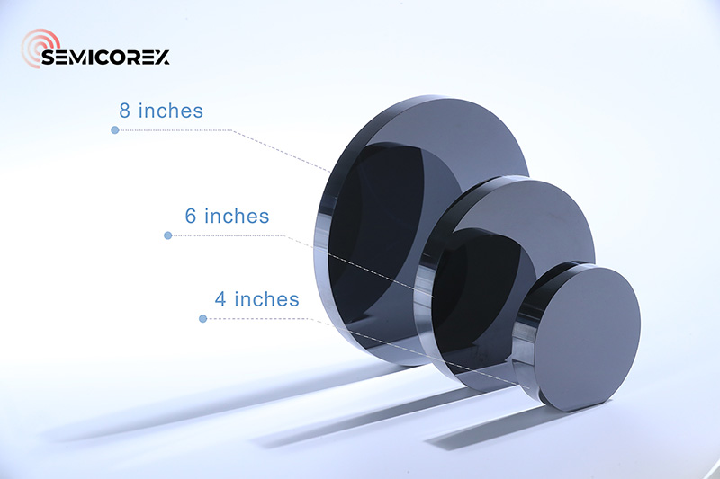
The PVT method is the primary method currently used in industrial production for growing SiC ingots. The surface and edges of the SiC ingots produced from the furnace are irregular. They must first undergo X-ray orientation, external rolling, and surface grinding to form smooth cylinders of standard dimensions. This allows for the critical step in ingot processing: slicing, which involves using precision cutting techniques to separate the SiC ingot into multiple thin slices.
Currently, the main slicing techniques include slurry wire cutting, diamond wire cutting, and laser lift-off. Slurry wire cutting uses abrasive wire and slurry to slice the SiC ingot. This is the most traditional method among several approaches. While cost-effective, it also suffers from slow cutting speeds and can leave deep damage layers on the substrate surface. These deep damage layers cannot be effectively removed even after subsequent grinding and CMP processes, and are easily inherited during the epitaxial growth process, resulting in defects such as scratches and step lines.
Diamond wire sawing uses diamond particles as an abrasive, rotating at high speeds to cut SiC ingots. This method offers fast cutting speeds and shallow surface damage, helping to improve substrate quality and yield. However, like slurry sawing, it also suffers from the significant SiC material loss. Laser lift-off, on the other hand, uses the thermal effects of a laser beam to separate SiC ingots, providing highly precise cuts and minimizing substrate damage, offering advantages in speed and loss.
After the aforementioned orientation, rolling, flattening, and sawing, the silicon carbide ingot becomes a thin crystal slice with minimal warpage and uniform thickness. Defects previously undetectable in the ingot can now be detected for preliminary in-process detection, providing crucial information for determining whether to proceed with wafer processing. The main defects detected are: stray crystals, micropipes, hexagonal voids, inclusions, abnormal color of small faces, polymorphism, etc. Qualified wafers are selected for the next step of SiC wafer processing.
Semicorex offers high-quality SiC ingots and wafers. If you have any inquiries or need additional details, please don't hesitate to get in touch with us.
Contact phone # +86-13567891907
Email: sales@semicorex.com


