- English
- Español
- Português
- русский
- Français
- 日本語
- Deutsch
- tiếng Việt
- Italiano
- Nederlands
- ภาษาไทย
- Polski
- 한국어
- Svenska
- magyar
- Malay
- বাংলা ভাষার
- Dansk
- Suomi
- हिन्दी
- Pilipino
- Türkçe
- Gaeilge
- العربية
- Indonesia
- Norsk
- تمل
- český
- ελληνικά
- український
- Javanese
- فارسی
- தமிழ்
- తెలుగు
- नेपाली
- Burmese
- български
- ລາວ
- Latine
- Қазақша
- Euskal
- Azərbaycan
- Slovenský jazyk
- Македонски
- Lietuvos
- Eesti Keel
- Română
- Slovenski
- मराठी
- Srpski језик
Precision ceramic components in semiconductor
Precision ceramic parts are key components of core equipment in key processes of semiconductor manufacturing, such as photolithography, etching, thin film deposition, ion implantation, CMP, etc., such as bearings, guide rails, liners, electrostatic chucks, mechanical handling arms, etc. Especially inside the equipment cavity, they play the functions of support, protection, and flow diversion.
In high-end lithography machines, in order to achieve high process precision, it is necessary to widely use ceramic components with good functional complexity, structural stability, thermal stability, and dimensional accuracy, such as electrostatic chuck, Vacuum-chuck, Block, magnetic steel skeleton water cooling plate, mirror, guide rail, workpiece table, mask table, etc.
Electrostatic chuck is a widely used silicon wafer clamping and transfer tool in semiconductor component manufacturing. It is widely used in plasma and vacuum-based semiconductor processes such as etching, chemical vapor deposition and ion implantation. The main ceramic materials are alumina ceramics and silicon nitride ceramics. The manufacturing difficulties are complex structural design, raw material selection and sintering, temperature control, and high-precision processing technology.
2. Mobile platform
The material system design of the mobile platform of the lithography machine is the key to the high precision and high speed of the lithography machine. In order to effectively resist the deformation of the mobile platform due to high-speed movement during the scanning process, the platform material should include low thermal expansion materials with high specific stiffness, that is, such materials should have high modulus and low density requirements. In addition, the material also needs a high specific stiffness, which enables the entire platform to maintain the same distortion level while withstanding higher acceleration and speed. By switching masks at a higher speed without increasing distortion, the throughput is increased, and the work efficiency is improved while ensuring high precision.
In order to transfer the chip circuit diagram from the mask to the wafer to achieve the predetermined chip function, the etching process is an important part. The components made of ceramic materials on the etching equipment mainly include the chamber, window mirror, gas dispersion plate, nozzle, insulation ring, cover plate, focusing ring and electrostatic chuck.
3. Chamber
As the minimum feature size of semiconductor devices continues to shrink, the requirements for wafer defects have become more stringent. In order to avoid contamination by metal impurities and particles, more stringent requirements have been put forward for the materials of semiconductor equipment cavities and components in the cavities. At present, ceramic materials have become the main materials for etching machine cavities.
Material requirements (1) High purity and low metal impurity content; (2) Stable chemical properties of the main components, especially low chemical reaction rate with halogen corrosive gases; (3) High density and few open pores; (4) Small grains and low grain boundary phase content; (5) Excellent mechanical properties and easy production and processing; (6) Some components may have other performance requirements, such as good dielectric properties, electrical conductivity or thermal conductivity.
4. Shower head
Its surface is densely distributed with hundreds or thousands of tiny through holes, like a precisely woven neural network, which can accurately control the gas flow and injection angle to ensure that every inch of wafer processing is evenly "bathed" in process gas, improving production efficiency and product quality.
Technical Difficulties In addition to the extremely high requirements for cleanliness and corrosion resistance, the gas distribution plate has strict requirements on the consistency of the aperture of the small holes on the gas distribution plate and the burrs on the inner wall of the small holes. If the aperture size tolerance and consistency standard deviation are too large or there are burrs on any inner wall, the thickness of the deposited film layer will be different, which will directly affect the equipment process yield.
5. Focus ring
The function of the focus ring is to provide balanced plasma, which requires a similar conductivity to the silicon wafer. In the past, the material used was mainly conductive silicon, but fluorine-containing plasma will react with silicon to generate volatile silicon fluoride, which greatly shortens its service life, resulting in frequent replacement of components and reduced production efficiency. SiC has similar conductivity to single-crystal Si, and has better resistance to plasma etching, so it can be used as a material for focusing rings.
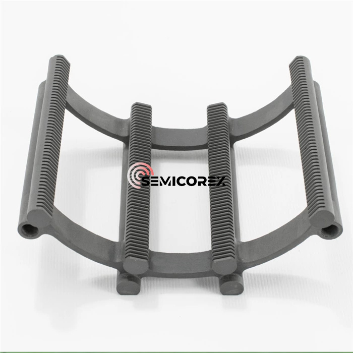
Semicorex offers high-quality ceramic parts in semiconductor industry. If you have any inquiries or need additional details, please don't hesitate to get in touch with us.
Contact phone # +86-13567891907
Email: sales@semicorex.com


