
- English
- Español
- Português
- русский
- Français
- 日本語
- Deutsch
- tiếng Việt
- Italiano
- Nederlands
- ภาษาไทย
- Polski
- 한국어
- Svenska
- magyar
- Malay
- বাংলা ভাষার
- Dansk
- Suomi
- हिन्दी
- Pilipino
- Türkçe
- Gaeilge
- العربية
- Indonesia
- Norsk
- تمل
- český
- ελληνικά
- український
- Javanese
- فارسی
- தமிழ்
- తెలుగు
- नेपाली
- Burmese
- български
- ລາວ
- Latine
- Қазақша
- Euskal
- Azərbaycan
- Slovenský jazyk
- Македонски
- Lietuvos
- Eesti Keel
- Română
- Slovenski
- मराठी
- Srpski језик

What are the differences between epitaxy and CVD
In the thin-film deposition process of chip manufacturing, two technologies are often mentioned together, yet they are fundamentally different—epitaxy and chemical vapor deposition. They are like cousins, both belonging to the "vapor growth" family, but with distinct characteristics and strengths. Sometimes, they are clearly separate; other times, they can transform into each other and coexist under specific conditions.
I. Fundamental Difference: One is Copying, the Other is Graffiti
Chemical Vapor Deposition (CVD) is the most common thin film deposition method. Its principle is simple: a gas containing the target element is introduced into a reaction chamber, where a chemical reaction occurs on the heated wafer surface, generating a solid thin film. CVD-generated films can be polycrystalline, amorphous, or single-crystalline, depending on the process conditions. It's like painting a wall—regardless of the wall's crystal structure, the paint simply solidifies into a film. CVD-deposited silicon dioxide, silicon nitride, polycrystalline silicon, etc., do not have strict lattice matching requirements with the substrate.
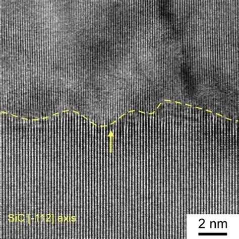
Epitaphing, on the other hand, is a "noble branch" in the CVD family. Its requirements are much more stringent: the deposited film must have the same crystal structure and orientation as the substrate, with atoms "growing" layer by layer to perfectly replicate the substrate's lattice arrangement. Epitaxy is like using the same template to copy bricks—the newly built wall must perfectly align the brick joints of the old wall. Epitaxial layers are typically single-crystalline silicon, germanium silicon, silicon carbide, etc., used to construct key structures such as the active region and heterojunctions of transistors.
Simply put, all epitaxy is CVD, but not all CVD is epitaxy. Epitaxy is a "single-crystal replication" mode of CVD achieved under specific conditions.
II. Differences in Process Conditions
CVD has a very wide process window. Temperatures can range from room temperature to thousands of degrees Celsius, pressures from atmospheric pressure to a few Pascals, and the types of gases are extremely diverse. Any process that allows a gas to react and form a solid thin film can be called CVD. Plasma-enhanced CVD can deposit silicon nitride at 300-400°C, low-pressure CVD at 600-700°C, and atmospheric pressure CVD at temperatures above 900°C, depositing silicon dioxide. CVD has almost no requirements for the substrate—silicon, glass, metals, and even plastics (under low-temperature conditions) can all be deposited.
Epitaphing, on the other hand, has a much narrower process window. To grow a perfect single-crystal layer, three stringent conditions must be met.
First, the substrate must be single-crystal. The epitaxial layer is a continuation of the substrate's crystal lattice; if the substrate itself is polycrystalline or amorphous, a single-crystal epitaxial layer cannot be grown.
Second, the temperature must be high enough. For silicon epitaxy, the temperature is typically 1000-1200°C; for silicon carbide epitaxy, the temperature can even reach 1500-1600°C. The high temperature provides sufficient surface mobility for the adsorbed atoms, allowing them to find their correct positions in the crystal lattice.
Third, the growth rate must be slow. Too fast a rate would cause the atoms to not have enough time to "line up," resulting in polycrystalline structures or defects. Typical growth rates for silicon epitaxy are 0.1-1 micrometers per minute, while CVD deposition of polycrystalline silicon can easily reach 10 micrometers per minute.
Furthermore, epitaxy requires extremely high cleanliness of the chamber; any impurity atom can become a defect center, compromising the integrity of the single crystal.
III. Interconversion
Under certain conditions, epitaxy and CVD can be interconverted.
From CVD to Epitaxy: If the substrate is monocrystalline silicon, and the deposition temperature is high enough and the growth rate is slow enough, the CVD process, which would normally produce polycrystalline silicon, can be transformed into monocrystalline epitaxy. For example, deposition with silane below 900°C yields polycrystalline silicon; raising the temperature to 1050°C while lowering the silane partial pressure allows for the growth of a monocrystalline epitaxial layer on a monocrystalline silicon substrate. This is the fundamental principle of epitaxial growth—by increasing the surface diffusion rate, atoms have the opportunity to "find" lattice positions.
From Epitaxy to CVD: If the temperature is not high enough, or the growth rate is too fast, the epitaxial process will "degenerate" into polycrystalline or amorphous deposition. For example, attempting to epitaxially grow silicon at low temperatures may result in amorphous silicon; epitaxy at high rates may introduce polycrystalline components. In industry, this "degradation" is sometimes deliberately used to grow polycrystalline silicon thin films. For example, in trench filling, a layer of amorphous silicon is first deposited at a low temperature as a buffer, and then annealed at a high temperature to crystallize it.
IV. Coexistence and Symbiosis
In advanced manufacturing processes, epitaxy and CVD often coexist in the same equipment, and even cooperate in the same process step.
Selective epitaxy is a typical example. In source-drain lift processes, epitaxial silicon needs to be selectively grown in exposed monocrystalline silicon regions, while nothing grows in silicon dioxide or silicon nitride isolation regions. This process is actually a "competition" between epitaxy and CVD—on the surface of monocrystalline silicon, atoms can migrate rapidly and find lattice positions to form an epitaxial layer; on insulating surfaces, atomic nucleation is slow, and the final deposited polycrystalline or amorphous material can be selectively etched away.
Continuous Deposition of Epitaxy and Polycrystalline: In 3D NAND manufacturing, sometimes it is necessary to first epitaxially grow monocrystalline silicon as a seed layer, and then switch to CVD mode to deposit polycrystalline silicon to fill trenches. The same epitaxial equipment can freely switch between monocrystalline and polycrystalline modes by adjusting the temperature and gas ratio.
Epitaxy + Deposition in Strained Silicon Technology: Germanium silicon is epitaxially grown in the source and drain regions of PMOS, and a silicon nitride stress pad is simultaneously CVD deposited on it. The two work together to introduce channel compressive stress and improve hole mobility.
V. Conclusion
Epitaxy and CVD represent two distinct approaches: one, the pursuit of "atomic-level perfect replication," and the other, the pragmatism of "efficient film formation." They share the fundamental principles of gas-phase chemical reactions, yet diverge significantly in terms of crystal quality, temperature window, and growth rate. By adjusting temperature and rate, they can be interconverted; through ingenious process design, they can coexist on a single device and work in the same process. It is this harmonious collaboration between these two cousins that allows chips to possess both perfect single-crystal channels and dense polycrystalline gates and insulating dielectric layers, supporting the magnificent edifice of billions of transistors working together.
Semicorex offers high-quality CVD coating products. If you have any inquiries or need additional details, please don't hesitate to get in touch with us.
Contact phone # +86-13567891907
Email: sales@semicorex.com


